Datasheet 搜索 > 逻辑芯片 > TI(德州仪器) > SN74LVC1G32DCKR 数据手册 > SN74LVC1G32DCKR 数据手册 12/38 页
 器件3D模型
¥ 0.189
SN74LVC1G32DCKR 数据手册 - TI(德州仪器)
制造商:
TI(德州仪器)
分类:
逻辑芯片
封装:
SC-70-5
描述:
TEXAS INSTRUMENTS SN74LVC1G32DCKR 或门, LVC系列, 1门, 2输入, 32 mA, 1.65V至5.5V, SC-70-5
Pictures:
3D模型
符号图
焊盘图
引脚图
产品图
页面导航:
引脚图在P3Hot
典型应用电路图在P11P12
原理图在P10
封装尺寸在P14P15P17P18
标记信息在P14P15
封装信息在P13P14P15P16P17P18
技术参数、封装参数在P4P11
应用领域在P1P16P38
电气规格在P6
型号编号列表在P11
导航目录
SN74LVC1G32DCKR数据手册
Page:
of 38 Go
若手册格式错乱,请下载阅览PDF原文件
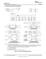
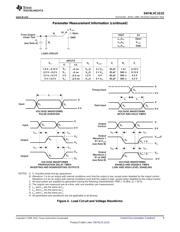
V
CC
Unused Input
Input
Output Output
Input
Unused Input
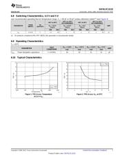
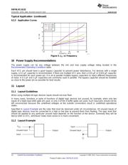
Frequency - MHz
Icc - mA
-20 0 20 40 60 80
-2
0
2
4
6
8
10
D003
Icc 1.8V
Icc 2.5V
Icc 3.3V
Icc 5V
SN74LVC1G32
SCES219V –APRIL 1999–REVISED AUGUST 2015
www.ti.com
Typical Application (continued)
9.2.3 Application Curves
Figure 5. I
CC
vs Frequency
10 Power Supply Recommendations
The power supply can be any voltage between the min and max supply voltage rating located in the
Recommended Operating Conditions table.
Each VCC pin should have a good bypass capacitor to prevent power disturbance. For devices with a single
supply, a 0.1-μF capacitor is recommended. If there are multiple VCC pins, then a 0.01-μF or 0.022-μF capacitor
is recommended for each power pin. It is ok to parallel multiple bypass capacitors to reject different frequencies
of noise. A 0.1-μF and 1-μF capacitors are commonly used in parallel. The bypass capacitor should be installed
as close to the power pin as possible for best results.
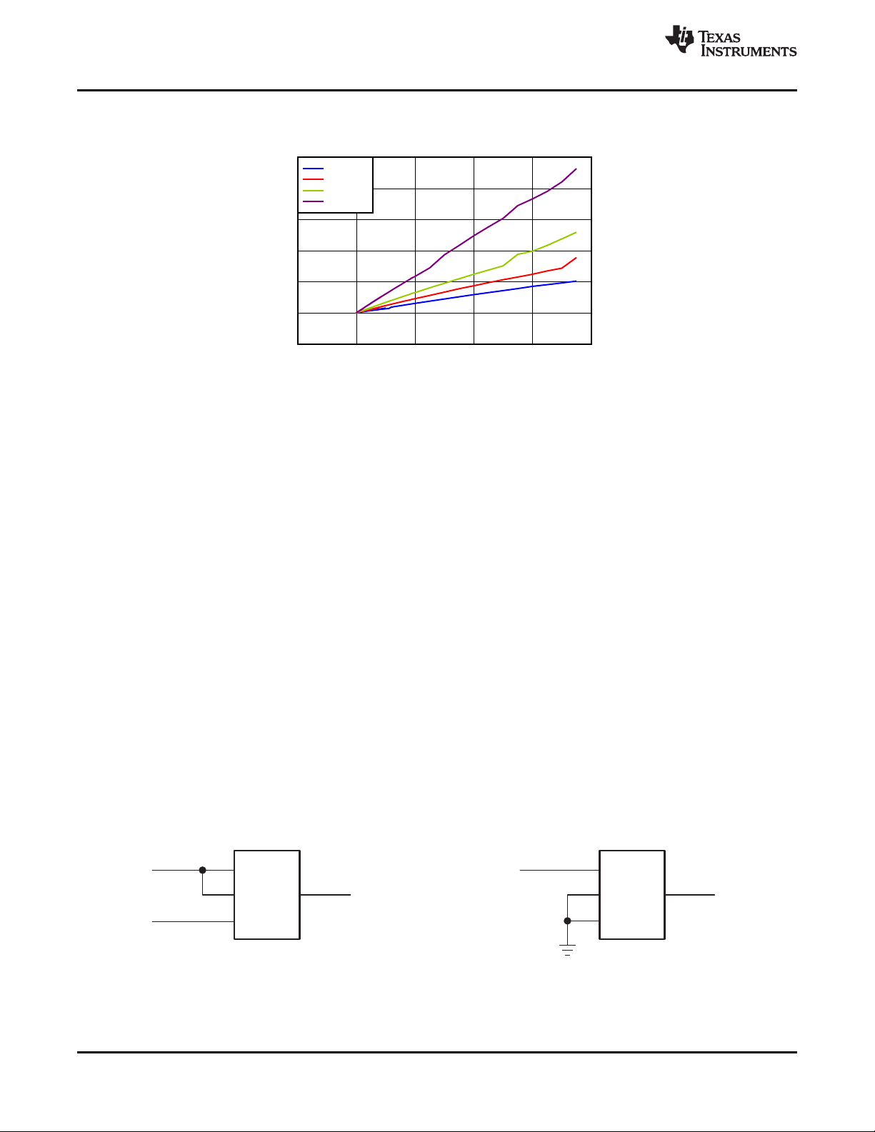
11 Layout
11.1 Layout Guidelines
When using multiple bit logic devices inputs should not ever float.
In many cases, functions or parts of functions of digital logic devices are unused; for example, when only two
inputs of a triple-input AND gate are used, or only 3 of the 4 buffer gates are used. Such input pins should not be
left unconnected because the undefined voltages at the outside connections result in undefined operational
states.
Specified in Layout Example are the rules that must be observed under all circumstances. All unused inputs of
digital logic devices must be connected to a high or low bias to prevent them from floating. The logic level that
should be applied to any particular unused input depends on the function of the device. Generally they will be
tied to GND or VCC, whichever make more sense or is more convenient.
11.2 Layout Example
12 Submit Documentation Feedback Copyright © 1999–2015, Texas Instruments Incorporated
Product Folder Links: SN74LVC1G32
器件 Datasheet 文档搜索
AiEMA 数据库涵盖高达 72,405,303 个元件的数据手册,每天更新 5,000 多个 PDF 文件
