Datasheet 搜索 > 逻辑芯片 > TI(德州仪器) > SN74LVC1G57DRLR 数据手册 > SN74LVC1G57DRLR 数据手册 1/26 页

¥ 0.919
SN74LVC1G57DRLR 数据手册 - TI(德州仪器)
制造商:
TI(德州仪器)
分类:
逻辑芯片
封装:
SOT-553-6
描述:
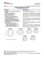
可配置多函数栅 CONFIGURABLE MULTIPLE-FUNCTION GATE
Pictures:
3D模型
符号图
焊盘图
引脚图
产品图
页面导航:
导航目录
SN74LVC1G57DRLR数据手册
Page:
of 26 Go
若手册格式错乱,请下载阅览PDF原文件
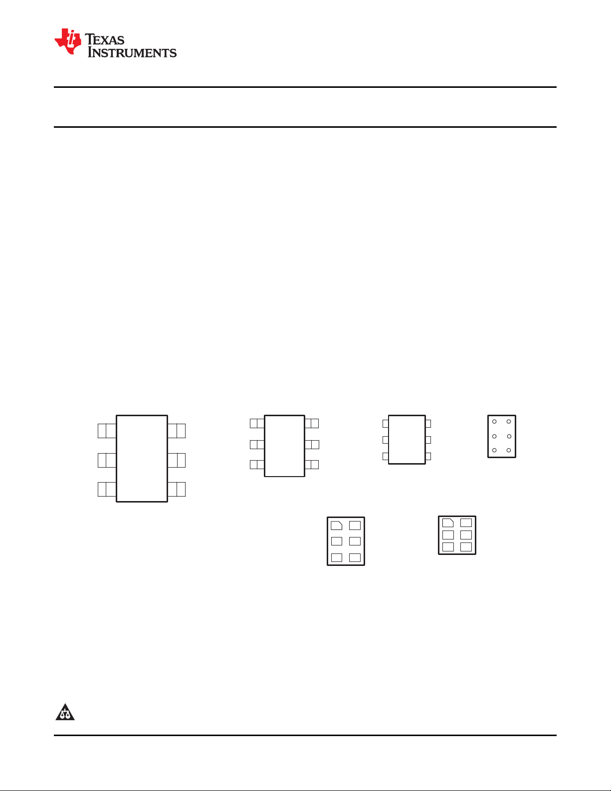
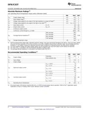
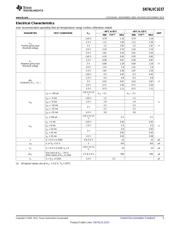
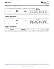
3
2
4
61
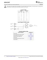
In1 In2
Y
GND
In0
DBV PACKAGE
(TOP VIEW)
YZP PACKAGE
(BOTTOM VIEW)
DCK PACKAGE
(TOP VIEW)
3
2
4
61
In1 In2
Y
GND
In0
3
2
4
61
In1 In2
Y
GND
In0
In1
In0
In2
Y
GND
DRL PACKAGE
(TOP VIEW)
See mechanical drawings for dimensions.
1
4
2
3
6
V
CC
V
CC
V
CC
5
V
CC
5
5
5
DRY PACKAGE
(TOP VIEW)
GND V
CC
ln1
6
5
4
2
3
ln0
Y
ln2
1
ln1
ln0
DSF PACKAGE
(TOP VIEW)
GND
ln2
Y
V
CC
6
5
4
2
3
1
SN74LVC1G57
www.ti.com
SCES414O –NOVEMBER 2002–REVISED DECEMBER 2013
Configurable Multiple-Function Gate
Check for Samples: SN74LVC1G57
1
FEATURES
DESCRIPTION
This configurable multiple-function gate is designed
2
• Available in the Texas Instruments NanoFree™
for 1.65-V to 5.5-V V
CC
operation.
Package
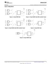
The SN74LVC1G57 device features configurable
• Supports 5-V V
CC
Operation
multiple functions. The output state is determined by
• Inputs Accept Voltages to 5.5 V
eight patterns of 3-bit input. The user can choose the
• Max t
pd
of 6.3 ns at 3.3 V
logic functions AND, OR, NAND, NOR, XNOR,
inverter, and noninverter. All inputs can be connected
• Supports Down Translation to V
CC
to V
CC
or GND.
• Low Power Consumption, 10-µA Max I
CC
This device functions as an independent gate, but
• ±24-mA Output Drive at 3.3 V
because of Schmitt action, it may have different input
• I
off
Supports Live Insertion, Partial-Power-
threshold levels for positive-going (V
T+
) and negative-
Down Mode, and Back-Drive Protection
going (V
T–
) signals.
• Latch-Up Performance Exceeds 100 mA Per
NanoFree™ package technology is a major
JESD 78, Class II
breakthrough in IC packaging concepts, using the die
• ESD Protection Exceeds JESD 22
as the package.
– 2000-V Human-Body Model (A114-A)
This device is fully specified for partial-power-down
– 200-V Machine Model (A115-A)
applications using I
off
. The I
off
circuitry disables the
outputs, preventing damaging current backflow
– 1000-V Charged-Device Model (C101)
through the device when it is powered down.
1
Please be aware that an important notice concerning availability, standard warranty, and use in critical applications of
Texas Instruments semiconductor products and disclaimers thereto appears at the end of this data sheet.
2NanoFree is a trademark of Texas Instruments.
PRODUCTION DATA information is current as of publication date.
Copyright © 2002–2013, Texas Instruments Incorporated
Products conform to specifications per the terms of the Texas
Instruments standard warranty. Production processing does not
necessarily include testing of all parameters.
器件 Datasheet 文档搜索
AiEMA 数据库涵盖高达 72,405,303 个元件的数据手册,每天更新 5,000 多个 PDF 文件
