Datasheet 搜索 > 逻辑芯片 > TI(德州仪器) > SN74LVC1G57DRY2 数据手册 > SN74LVC1G57DRY2 数据手册 1/31 页

¥ 0.926
SN74LVC1G57DRY2 数据手册 - TI(德州仪器)
制造商:
TI(德州仪器)
分类:
逻辑芯片
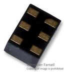
封装:
UFDFN-6
描述:
可配置多函数栅 CONFIGURABLE MULTIPLE-FUNCTION GATE
Pictures:
3D模型
符号图
焊盘图
引脚图
产品图
页面导航:
引脚图在P3Hot
典型应用电路图在P1P10P11
原理图在P8
封装尺寸在P14P16P17P24
焊盘布局在P25
标记信息在P14P15
封装信息在P13P14P15P16P17
技术参数、封装参数在P4
应用领域在P1
电气规格在P5P6
导航目录
SN74LVC1G57DRY2数据手册
Page:
of 31 Go
若手册格式错乱,请下载阅览PDF原文件
Copyright © 2016, Texas Instruments Incorporated
Product
Folder
Sample &
Buy
Technical
Documents
Tools &
Software
Support &
Community
An IMPORTANT NOTICE at the end of this data sheet addresses availability, warranty, changes, use in safety-critical applications,
intellectual property matters and other important disclaimers. PRODUCTION DATA.
SN74LVC1G57
SCES414P –NOVEMBER 2002–REVISED NOVEMBER 2016
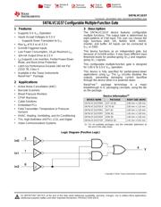
SN74LVC1G57 Configurable Multiple-Function Gate
1
1 Features
1
• Supports 5-V V
CC
Operation
• Inputs Accept Voltages to 5.5 V
– Supports Down Translation to V
CC
• Max t
pd
of 6.3 ns at 3.3 V
• Schmitt-Triggered Inputs
• Low Power Consumption, 10-µA Maximum I
CC
• ±24-mA Output Drive at 3.3 V
• I
off
Supports Live Insertion, Partial-Power-Down
Mode, and Back-Drive Protection
• Latch-Up Performance Exceeds 100 mA Per
JESD 78, Class II
• Available in the Texas Instruments
NanoFree™ Package
2 Applications
• Active Noise Cancellation (ANC)
• Barcode Scanners
• Blood Pressure Monitors
• CPAP Machines
• Cable Solutions
• Embedded PCs
• Field Transmitter: Temperature or Pressure
Sensors
• HVAC: Heating, Ventilating, and Air Conditioning
• TVs: High-Definition (HDTV), LCD, and Digital
• Video Communications Systems
3 Description
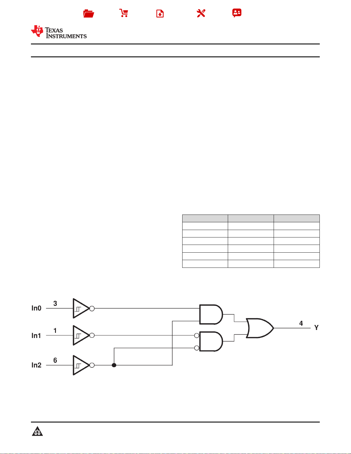
The SN74LVC1G57 device features configurable
multiple functions. The output state is determined by
eight patterns of 3-bit input. The user can choose the
logic functions AND, OR, NAND, NOR, XNOR,
inverter, and buffer. All inputs can be connected to
V
CC
or GND.
This device functions as an independent gate, but
because of Schmitt action, it may have different input
threshold levels for positive-going (V
T+
) and negative-
going (V
T–
) signals.
This configurable multiple-function gate is designed
for 1.65-V to 5.5-V V
CC
operation.
This device is fully specified for partial-power-down
applications using I
off
. The I
off
circuitry disables the
outputs, preventing damaging current backflow
through the device when it is powered down.
NanoFree™ package technology is a major
breakthrough in IC packaging concepts, using the die
as the package.
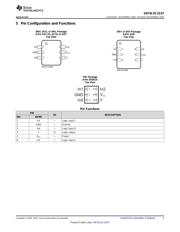
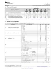
Device Information
(1)
DEVICE NAME PACKAGE BODY SIZE (NOM)
SN74LVC1G57DBV SOT-23 (6) 2.90 mm × 1.60 mm
SN74LVC1G57DCK SC70 (6) 2.00 mm × 1.25 mm
SN74LVC1G57DRL SOT (6) 1.60 mm × 1.20 mm
SN74LVC1G57DRY SON (6) 1.45 mm × 1.00 mm
SN74LVC1G57DSF SON (6) 1.00 mm × 1.00 mm
SN74LVC1G57YZP DSBGA (6) 1.41 mm × 0.91 mm
(1) For all available packages, see the orderable addendum at
the end of the data sheet.
Logic Diagram (Positive Logic)
器件 Datasheet 文档搜索
AiEMA 数据库涵盖高达 72,405,303 个元件的数据手册,每天更新 5,000 多个 PDF 文件
