Datasheet 搜索 > 逻辑控制器 > TI(德州仪器) > SN74LVC244ADGVR 数据手册 > SN74LVC244ADGVR 数据手册 1/31 页
 器件3D模型
¥ 0.915
SN74LVC244ADGVR 数据手册 - TI(德州仪器)
制造商:
TI(德州仪器)
分类:
逻辑控制器
封装:
TVSOP-20
描述:
74LVC 系列反相器和缓冲器,德州仪器德州仪器的 74LVC 系列低功率 CMOS 逻辑集 IC 的一系列反相器和缓冲器。 74LVC 系列使用硅门 CMOS 技术,设计用于在 3.3V 时工作,与 5V 系统相比,允许功耗显著降低。工作电压:1.65 至 3.6V 5V 容差的输入 兼容性:输入 LVTTL/TTL,输出 LVCMOS 按 JESD 17标准,闩锁效应性能超过 250 mA ESD 保护超过 JESD 22 ### 74LVC 系列
Pictures:
3D模型
符号图
焊盘图
引脚图
产品图
页面导航:
引脚图在P3Hot
典型应用电路图在P10P11
原理图在P1P9P10
封装尺寸在P13P14P16P17
标记信息在P13P14P15
封装信息在P12P13P14P15P16P17
技术参数、封装参数在P4P10
应用领域在P1P31
电气规格在P6
型号编号列表在P10
导航目录
SN74LVC244ADGVR数据手册
Page:
of 31 Go
若手册格式错乱,请下载阅览PDF原文件
1
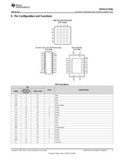
2 18
1Y1
1OE
1A1
4 16
1Y2
1A2
6 14
1Y3
1A3
8 12
1Y4
1A4
19
11 9
2Y1
2OE
2A1
13 7
2Y2
2A2
15 5
2Y3
2A3
17 3
2Y4
2A4
Pin numbers shown are for the DB, DGV, DW, N, NS, PW, and RGY packages.
Product
Folder
Sample &
Buy
Technical
Documents
Tools &
Software
Support &
Community
SN74LVC244A
SCAS414Z –NOVEMBER 1992–REVISED JANUARY 2015
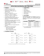
SN74LVC244A Octal Buffer/Driver With 3-State Outputs
1 Features 2 Applications
1
• Operates From 1.65 V to 3.6 V
• Servers
• Inputs Accept Voltages to 5.5 V • LED Displays
• Specified From –40°C to 85°C and • Network Switches
–40°C to 125°C
• Telecom Infrastructure
• Max t
pd
of 5.9 ns at 3.3 V
• Motor Drivers
• Typical V
OLP
(Output Ground Bounce)
• I/O Expanders
< 0.8 V at V
CC
= 3.3 V, T
A
= 25°C
3 Description
• Typical V
OHV
(Output V
OH
Undershoot)
> 2 V at V
CC
= 3.3 V, T
A
= 25°C
These octal bus buffers are designed for 1.65-V to
3.6-V VCC operation. The ’LVC244A devices are
• Supports Mixed-Mode Signal Operation on
designed for asynchronous communication between
All Ports (5-V Input/Output Voltage With
data buses.
3.3-V V
CC
)
• I
off
Supports Live Insertion, Partial-Power-Down
Device Information
(1)
Mode, and Back-Drive Protection
PART NUMBER PACKAGE (PIN) BODY SIZE
• Can Be Used as a Down Translator to Translate
PDIP (20) 25.40 mm x 6.35 mm
Inputs From a Max of 5.5 V Down
SOP (20) 12.60 mm x 5.30 mm
to the V
CC
Level
SN74LVC244A SSOP (20) 7.50 mm x 5.30 mm
• Latch-Up Performance Exceeds 250 mA Per
TVSOP (20) 5.00 mm x 4.40 mm
JESD 17
SOIC (20) 12.80 mm x 7.50 mm
• ESD Protection Exceeds JESD 22
(1) For all available packages, see the orderable addendum at
the end of the data sheet.
– 2000-V Human-Body Model
– 200-V Machine Model
– 1000-V Charged-Device Model
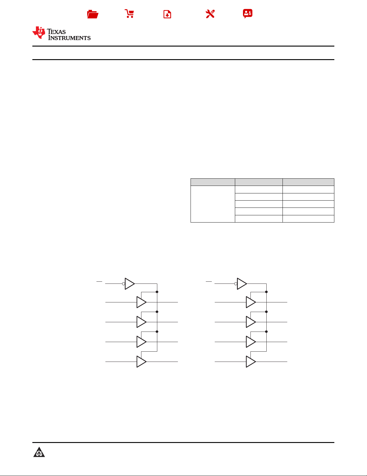
4 Simplified Schematic
1
An IMPORTANT NOTICE at the end of this data sheet addresses availability, warranty, changes, use in safety-critical applications,
intellectual property matters and other important disclaimers. PRODUCTION DATA.
器件 Datasheet 文档搜索
AiEMA 数据库涵盖高达 72,405,303 个元件的数据手册,每天更新 5,000 多个 PDF 文件
