Datasheet 搜索 > 逻辑芯片 > TI(德州仪器) > SN74LVC2G04DBVT 数据手册 > SN74LVC2G04DBVT 数据手册 4/26 页

¥ 5.024
SN74LVC2G04DBVT 数据手册 - TI(德州仪器)
制造商:
TI(德州仪器)
分类:
逻辑芯片
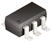
封装:
SOT-23-6
描述:
74LVC2G 系列,Texas Instruments### 74LVC 系列
Pictures:
3D模型
符号图
焊盘图
引脚图
产品图
页面导航:
引脚图在P3Hot
典型应用电路图在P1P9P10
原理图在P8P9
封装尺寸在P13P15P16P23
焊盘布局在P24
标记信息在P13P14
封装信息在P3P12P13P14P15P16
技术参数、封装参数在P4P9
应用领域在P1P14P26
电气规格在P5
型号编号列表在P9
导航目录
SN74LVC2G04DBVT数据手册
Page:
of 26 Go
若手册格式错乱,请下载阅览PDF原文件
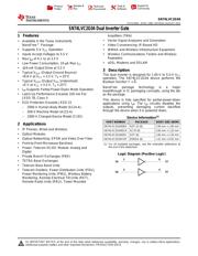
SN74LVC2G04
SCES195N –APRIL 1999–REVISED AUGUST 2015
www.ti.com
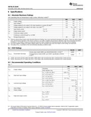
6 Specifications
6.1 Absolute Maximum Ratings
over operating free-air temperature range (unless otherwise noted)
(1)
MIN MAX UNIT
V
CC
Supply voltage –0.5 6.5 V
V
I
Input voltage
(2)
–0.5 6.5 V
V
O
Voltage applied to any output in the high-impedance or power-off state
(2)
–0.5 6.5 V
V
O
Voltage applied to any output in the high or low state
(2)(3)
–0.5 V
CC
+ 0.5 V
I
IK
Input clamp current V
I
< 0 –50 mA
I
OK
Output clamp current V
O
< 0 –50 mA
I
O
Continuous output current ±50 mA
Continuous current through V
CC
or GND ±100 mA
T
stg
Storage temperature –65 150 °C
(1) Stresses beyond those listed under Absolute Maximum Ratings may cause permanent damage to the device. These are stress ratings
only, and functional operation of the device at these or any other conditions beyond those indicated under Recommended Operating
Conditions is not implied. Exposure to absolute-maximum-rated conditions for extended periods may affect device reliability.
(2) The input negative-voltage and output voltage ratings may be exceeded if the input and output current ratings are observed.
(3) The value of V
CC
is provided in the recommended operating conditions table.
6.2 ESD Ratings
VALUE UNIT
Human body model (HBM), per ANSI/ESDA/JEDEC JS-001
(1)
+2000
V
(ESD)
Electrostatic discharge V
Charged-device model (CDM), per JEDEC specification JESD22-
+1000
C101
(2)
(1) JEDEC document JEP155 states that 500-V HBM allows safe manufacturing with a standard ESD control process.
(2) JEDEC document JEP157 states that 250-V CDM allows safe manufacturing with a standard ESD control process.
6.3 Recommended Operating Conditions
See
(1)
.
MIN MAX UNIT
Operating 1.65 5.5
V
CC
Supply voltage V
Data retention only 1.5
V
CC
= 1.65 V to 1.95 V 0.65 × V
CC
V
CC
= 2.3 V to 2.7 V 1.7
V
IH
High-level input voltage V
V
CC
= 3 V to 3.6 V 2
V
CC
= 4.5 V to 5.5 V 0.7 × V
CC
V
CC
= 1.65 V to 1.95 V 0.35 × V
CC
V
CC
= 2.3 V to 2.7 V 0.7
V
IL
Low-level input voltage V
V
CC
= 3 V to 3.6 V 0.8
V
CC
= 4.5 V to 5.5 V 0.3 × V
CC
V
I
Input voltage 0 5.5 V
V
O
Output voltage 0 V
CC
V
V
CC
= 1.65 V –4
V
CC
= 2.3 V –8
I
OH
High-level output current –16 mA
V
CC
= 3 V
–24
V
CC
= 4.5 V –32
(1) All unused inputs of the device must be held at V
CC
or GND to ensure proper device operation. Refer to the TI application report,
Implications of Slow or Floating CMOS Inputs, literature number SCBA004.
4 Submit Documentation Feedback Copyright © 1999–2015, Texas Instruments Incorporated
Product Folder Links: SN74LVC2G04
器件 Datasheet 文档搜索
AiEMA 数据库涵盖高达 72,405,303 个元件的数据手册,每天更新 5,000 多个 PDF 文件
