Datasheet 搜索 > 逻辑芯片 > TI(德州仪器) > SN74LVC2G07MDCKTEP 数据手册 > SN74LVC2G07MDCKTEP 数据手册 1/11 页
 器件3D模型
¥ 15.925
SN74LVC2G07MDCKTEP 数据手册 - TI(德州仪器)
制造商:
TI(德州仪器)
分类:
逻辑芯片
封装:
SC-70-6
描述:
具有漏极开路输出的增强型产品双路缓冲器/驱动器 6-SC70 -55 to 125
Pictures:
3D模型
符号图
焊盘图
引脚图
产品图
页面导航:
封装尺寸在P6P8P9
标记信息在P6
封装信息在P6P7P8P9
应用领域在P11
导航目录
SN74LVC2G07MDCKTEP数据手册
Page:
of 11 Go
若手册格式错乱,请下载阅览PDF原文件
1
FEATURES
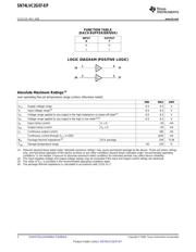
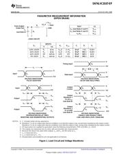
Seemechanicaldrawingsfordimensions.
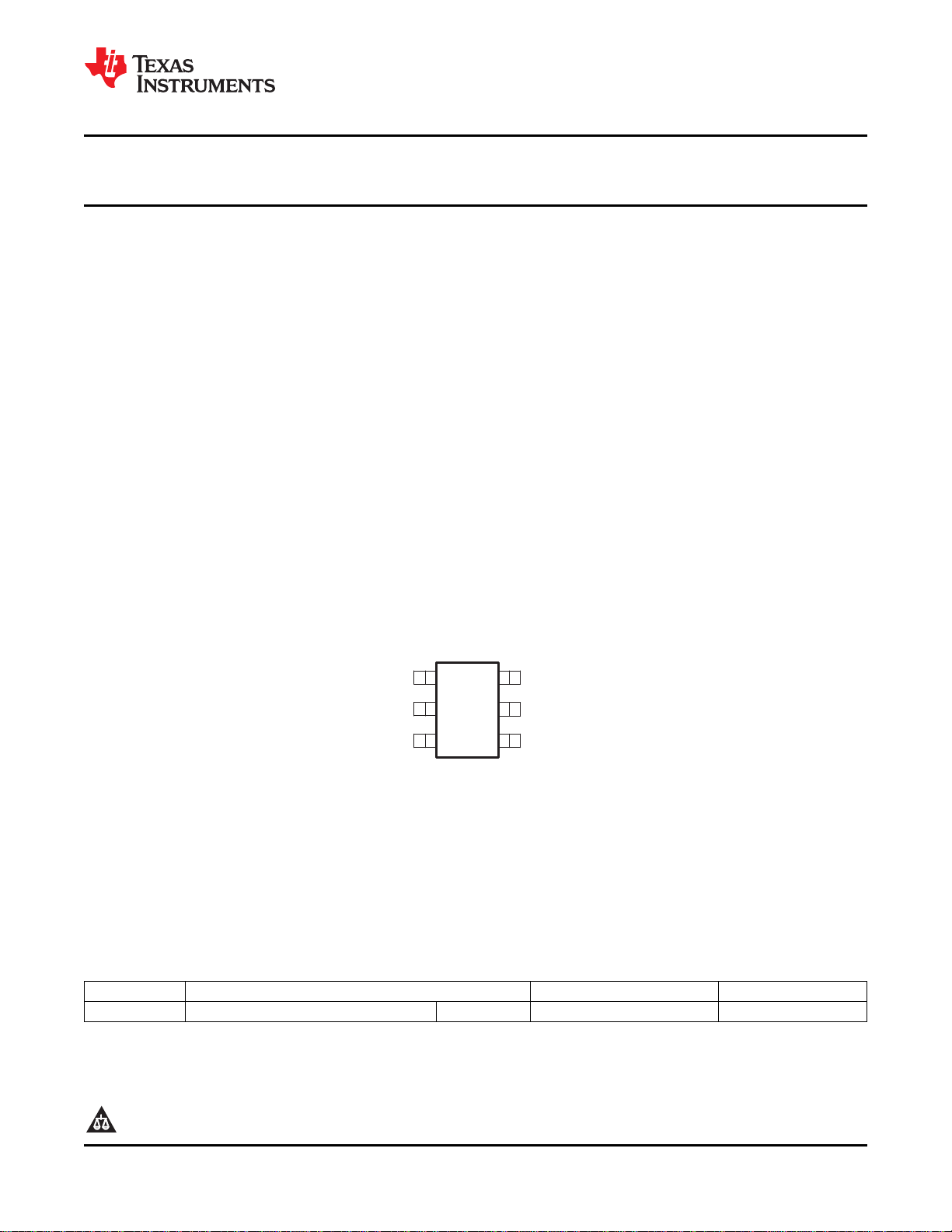
DCKPACKAGE
(TOP VIEW)
3
4
2A
2
GND
2Y
5
1
1A
V
CC
6
1Y
DESCRIPTION/ORDERING INFORMATION
SN74LVC2G07-EP
www.ti.com
....................................................................................................................................................................................................... SCES719 – MAY 2008
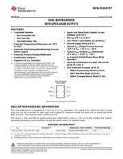
DUAL BUFFER/DRIVER
WITH OPEN-DRAIN OUTPUTS
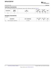
• Controlled Baseline • Inputs and Open-Drain Outputs Accept
Voltages up to 5.5 V
– One Assembly Site
• Max t
pd
of 5.7 ns at 3.3 V
– One Test Site
• Low Power Consumption, 10 µ A Max I
CC
– One Fabrication Site
• ± 24-mA Output Drive at 3.3 V
• Extended Temperature Performance of – 55 ° C
to 125 ° C • Typical V
OLP
(Output Ground Bounce)
<0.8 V at V
CC
= 3.3 V, T
A
= 25 ° C
• Enhanced Diminishing Manufacturing Sources
(DMS) Support • Typical V
OHV
(Output V
OH
Undershoot)
>2 V at V
CC
= 3.3 V, T
A
= 25 ° C
• Enhanced Product-Change Notification
• I
off
Supports Partial-Power-Down Mode
• Qualification Pedigree
(1)
Operation
• Supports 5-V V
CC
Operation
• Latch-Up Performance Exceeds 100 mA Per
(1) Component qualification in accordance with JEDEC and
JESD 78, Class II
industry standards to ensure reliable operation over an
extended temperature range. This includes, but is not limited
• ESD Protection Exceeds JESD 22
to, Highly Accelerated Stress Test (HAST) or biased 85/85,
temperature cycle, autoclave or unbiased HAST,
– 2000-V Human-Body Model (A114-A)
electromigration, bond intermetallic life, and mold compound
– 200-V Machine Model (A115-A)
life. Such qualification testing should not be viewed as
justifying use of this component beyond specified
– 1000-V Charged-Device Model (C101)
performance and environmental limits.
This dual buffer/driver is designed for 1.65-V to 5.5-V V
CC
operation. The output of the SN74LVC2G07 is open
drain and can be connected to other open-drain outputs to implement active low wired OR or active high wired
AND functions. The maximum sink current is 32 mA.
This device is fully specified for partial power-down applications using I
off
. The I
off
circuitry disables the outputs,
preventing damaging current backflow through the device when it is powered down.
ORDERING INFORMATION
(1)
T
A
PACKAGE
(2)
ORDERABLE PART NUMBER TOP-SIDE MARKING
– 55 ° C to 125 ° C SOT (SC-70) – DCK Reel of 250 SN74LVC2G07MDCKTEP CHC
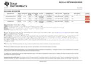
(1) For the most current package and ordering information, see the Package Option Addendum at the end of this document, or see the TI
website at www.ti.com .
(2) Package drawings, thermal data, and symbolization are available at www.ti.com/packaging .
1
Please be aware that an important notice concerning availability, standard warranty, and use in critical applications of
Texas Instruments semiconductor products and disclaimers thereto appears at the end of this data sheet.
PRODUCTION DATA information is current as of publication date.
Copyright © 2008, Texas Instruments Incorporated
Products conform to specifications per the terms of the Texas
Instruments standard warranty. Production processing does not
necessarily include testing of all parameters.
器件 Datasheet 文档搜索
AiEMA 数据库涵盖高达 72,405,303 个元件的数据手册,每天更新 5,000 多个 PDF 文件
