Datasheet 搜索 > 逻辑控制器 > TI(德州仪器) > SN74LVC2G07YZPR 数据手册 > SN74LVC2G07YZPR 数据手册 1/27 页
 器件3D模型
¥ 1.115
SN74LVC2G07YZPR 数据手册 - TI(德州仪器)
制造商:
TI(德州仪器)
分类:
逻辑控制器
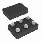
封装:
DSBGA-6
描述:
双缓冲/驱动器,具有漏极开路输出 DUAL BUFFER/DRIVER WITH OPEN-DRAIN OUTPUTS
Pictures:
3D模型
符号图
焊盘图
引脚图
产品图
页面导航:
引脚图在P3Hot
典型应用电路图在P9P10
原理图在P1P8
封装尺寸在P12P14P15P24
焊盘布局在P25
标记信息在P12P13
封装信息在P11P12P13P14P15
技术参数、封装参数在P4P9
应用领域在P1P13
电气规格在P5
型号编号列表在P9
导航目录
SN74LVC2G07YZPR数据手册
Page:
of 27 Go
若手册格式错乱,请下载阅览PDF原文件
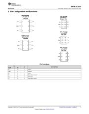
1A 1Y
1 6
2A 2Y
3 4
Product
Folder
Order
Now
Technical
Documents
Tools &
Software
Support &
Community
An IMPORTANT NOTICE at the end of this data sheet addresses availability, warranty, changes, use in safety-critical applications,
intellectual property matters and other important disclaimers. PRODUCTION DATA.
SN74LVC2G07
SCES308L –AUGUST 2001–REVISED MAY 2015
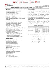
SN74LVC2G07 Dual Buffer and Driver With Open-Drain Outputs
1
1 Features
1
• Dual Open-Drain Buffer Configuration
• -24-mA Output Drive at 3.3 V
• Support Translation-Up and Down
• Available in the Texas Instruments
NanoFree™ Package
• Supports 5-V V
CC
Operation
• Inputs and Open-Drain Outputs Accept Voltages
Up to 5.5 V
• Max t
pd
of 3.7 ns at 3.3 V
• Low Power Consumption, 10-μA Max I
CC
• Typical V
OLP
(Output Ground Bounce)
<0.8 V at V
CC
= 3.3 V, T
A
= 25 ° C
• Typical V
OHV
(Output V
OH
Undershoot)
>2 V at V
CC
= 3.3 V, T
A
= 25 ° C
• I
off
Supports Live Insertion, Partial-Power-Down
Mode, and Back-Drive Protection
• Latch-Up Performance Exceeds 100 mA
Per JESD 78, Class II
• ESD Protection Exceeds JESD 22
– 2000-V Human-Body Model (A114-A)
– 200-V Machine Model (A115-A)
– 1000-V Charged-Device Model (C101)
2 Applications
• Blu-ray Players and Home Theaters
• DVD Recorders and Players
• Desktops or Notebook PCs
• Digital Video Cameras (DVC)
• Embedded PCs
• GPS: Personal Navigation Devices
• Mobile Phones
• Network Projector Front Ends
• Portable Media Players
• Solid State Drive (SSD): Enterprise
• High-Definition (HDTV)
• Tablet: Enterprise
• Audio Dock: Portable
• DLP Front Projection System
3 Description
This dual buffer and driver is designed for 1.65-V to
5.5-V V
CC
operation. The output of the
SN74LVC2G07 device is open drain and can be
connected to other open-drain outputs to implement
active-low wired-OR or active-high wired-AND
functions. The maximum sink current is 32 mA.
NanoFree package technology is a major
breakthrough in IC packaging concepts, using the die
as the package.
This device is fully specified for partial-power-down
applications using I
off
. The I
off
circuitry disables the
outputs, preventing damaging current backflow
through the device when it is powered down.
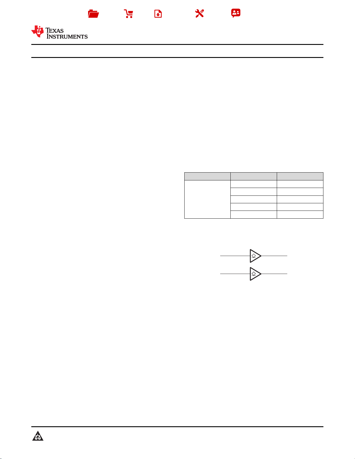
Device Information
(1)
PART NUMBER PACKAGE BODY SIZE (NOM)
SN74LVC2G07
SOT-23 (6) 2.90 mm × 1.60 mm
SC70 (6) 2.00 mm × 1.25 mm
DRY SON (6) 1.45 mm × 1.00 mm
DSF SON (6) 1.00 mm × 1.00 mm
DSBGA (6) 1.41 mm × 0.91 mm
(1) For all available packages, see the orderable addendum at
the end of the datasheet.
Functional Block Diagram
器件 Datasheet 文档搜索
AiEMA 数据库涵盖高达 72,405,303 个元件的数据手册,每天更新 5,000 多个 PDF 文件
