Datasheet 搜索 > 接口芯片 > TI(德州仪器) > SN75LBC176AP 数据手册 > SN75LBC176AP 数据手册 3/20 页

 器件3D模型
¥ 32.281
SN75LBC176AP 数据手册 - TI(德州仪器)
制造商:
TI(德州仪器)
分类:
接口芯片
封装:
PDIP-8
描述:
差分总线收发器 DIFFERENTIAL BUS TRANSCEIVERS
Pictures:
3D模型
符号图
焊盘图
引脚图
产品图
页面导航:
封装尺寸在P13P15P16
标记信息在P13P14
封装信息在P13P14P15P16
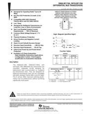
应用领域在P1P14P20
导航目录
SN75LBC176AP数据手册
Page:
of 20 Go
若手册格式错乱,请下载阅览PDF原文件
SLLS376D− MAY 2000 − REVISED JULY 2008
3
POST OFFICE BOX 655303 • DALLAS, TEXAS 75265
POST OFFICE BOX 1443
• HOUSTON, TEXAS 77251−1443
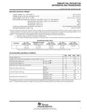
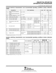
absolute maximum ratings
†
Supply voltage, V
CC
(see Note 1) −0.3 V to 6 V. . . . . . . . . . . . . . . . . . . . . . . . . . . . . . . . . . . . . . . . . . . . . . . . . . . .
Voltage range at any bus terminal (A or B) −10 V to 15 V. . . . . . . . . . . . . . . . . . . . . . . . . . . . . . . . . . . . . . . . . . . .
Input voltage, V
I
(D, DE, R, or RE) −0.3 V to V
CC
+ 0.5 V. . . . . . . . . . . . . . . . . . . . . . . . . . . . . . . . . . . . . . . . . . . .
Electrostatic discharge:Bus terminals and GND, Class 3, A: (see Note 2) 12 kV. . . . . . . . . . . . . . . . . . . . . . . .
Bus terminals and GND, Class 3, B: (see Note 2) 400 V. . . . . . . . . . . . . . . . . . . . . . . .
All terminals, Class 3, A: 3 kV. . . . . . . . . . . . . . . . . . . . . . . . . . . . . . . . . . . . . . . . . . . . . . .
All terminals, Class 3, B: 400 V. . . . . . . . . . . . . . . . . . . . . . . . . . . . . . . . . . . . . . . . . . . . .
Continuous total power dissipation (see Note 3) See Dissipation Rating Table. . . . . . . . . . . . . . . . . . . . . . . . . .
Storage temperature range, T
stg
−65°C to 150°C. . . . . . . . . . . . . . . . . . . . . . . . . . . . . . . . . . . . . . . . . . . . . . . . . . .
†
Stresses beyond those listed under “absolute maximum ratings” may cause permanent damage to the device. These are stress ratings only, and
functional operation of the device at these or any other conditions beyond those indicated under “recommended operating conditions” is not
implied. Exposure to absolute-maximum-rated conditions for extended periods may affect device reliability.
NOTES: 1. All voltage values, except differential I/O bus voltage, are with respect to network ground terminal.
2. Tested in accordance with MIL−STD−883C, Method 3015.7
3. The maximum operating junction temperature is internally limited. Use the dissipation rating table to operate below this temperature.
DISSIPATION RATING TABLE
PACKAGE
T
A
≤ 25°C
POWER RATING
DERATING FACTOR
‡
ABOVE T
A
= 25°C
T
A
= 70°C
POWER RATING
T
A
= 85°C
POWER RATING
T
A
= 125°C
POWER RATING
D 725 mW 5.8 mW/°C 464 mW 377 mW 145 mW
P 1000 mW 8.0 mW/°C 640 mW 520 mW —
‡
This is the inverse of the junction-to-ambient thermal resistance when board-mounted and with no air flow.
recommended operating conditions
MIN NOM MAX UNIT
Supply voltage, V
CC
4.75 5 5.25 V
Voltage at any bus terminal (separately or common mode), V
I
or V
IC
−7 12 V
High-level input voltage, V
IH
D, DE, and RE 2 V
CC
V
Low-level input voltage, V
IL
D, DE, and RE 0 0.8 V
Differential input voltage, V
ID
(see Note 4) −12
§
12 V
High-level output current, I
OH
Driver −60
mA
High-level output current, I
OH
Receiver −8
mA
Low-level output current, I
OL
Driver 60
mA
Low-level output current, I
OL
Receiver 8
mA
SN65LBC176AQ −40 125
Operating free-air temperature, T
A
SN65LBC176A −40 85
°C
Operating free-air temperature, T
A
SN75LBC176A 0 70
C
§
The algebraic convention, in which the least positive (most negative) limit is designated as minimum, is used in this data sheet.
NOTE 4: Differential input/output bus voltage is measured at the noninverting terminal A with respect to the inverting terminal B.
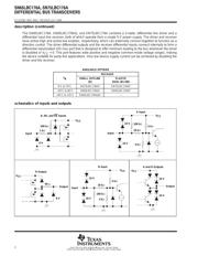
器件 Datasheet 文档搜索
AiEMA 数据库涵盖高达 72,405,303 个元件的数据手册,每天更新 5,000 多个 PDF 文件
