Datasheet 搜索 > 微控制器 > ST Microelectronics(意法半导体) > STM32F100RBT6B 数据手册 > STM32F100RBT6B 数据手册 29/95 页
 器件3D模型
¥ 16.51
STM32F100RBT6B 数据手册 - ST Microelectronics(意法半导体)
制造商:
ST Microelectronics(意法半导体)
分类:
微控制器
封装:
LQFP-64
描述:
STMICROELECTRONICS STM32F100RBT6B 微控制器, 32位, 线路接入, ARM 皮质-M3, 24 MHz, 128 KB, 8 KB, 64 引脚, LQFP
Pictures:
3D模型
符号图
焊盘图
引脚图
产品图
页面导航:
引脚图在P22P23P24P25P26P27P28P29Hot
典型应用电路图在P48P50P71
封装尺寸在P76
型号编码规则在P89P90P91
封装信息在P76P77P78P79P80P81P82P83P84P85P86P87
技术参数、封装参数在P33P55
电气规格在P31P32P33P34P35P36P37P38P39P40P41P42
导航目录
STM32F100RBT6B数据手册
Page:
of 95 Go
若手册格式错乱,请下载阅览PDF原文件

DocID16455 Rev 8 29/95
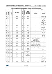
STM32F100x4, STM32F100x6, STM32F100x8, STM32F100xB Pinouts and pin description
94
1. I = input, O = output, S = supply, HiZ= high impedance.
2. FT= 5 V tolerant.
3. Function availability depends on the chosen device. For devices having reduced peripheral counts, it is always the lower
number of peripherals that is included. For example, if a device has only one SPI, two USARTs and two timers, they will be
called SPI1, USART1 & USART2 and TIM2 & TIM 3, respectively. Refer to Table 2 on page 11.
4. If several peripherals share the same I/O pin, to avoid conflict between these alternate functions only one peripheral should
be enabled at a time through the peripheral clock enable bit (in the corresponding RCC peripheral clock enable register).
5. PC13, PC14 and PC15 are supplied through the power switch and since the switch only sinks a limited amount of current
(3 mA), the use of GPIOs PC13 to PC15 in output mode is restricted: the speed should not exceed 2 MHz with a maximum
load of 30 pF and these IOs must not be used as a current source (e.g. to drive an LED).
6. Main function after the first backup domain power-up. Later on, it depends on the contents of the Backup registers even
after reset (because these registers are not reset by the main reset). For details on how to manage these IOs, refer to the
Battery backup domain and BKP register description sections in the STM32F10xxx reference manual, available from the
STMicroelectronics website: www.st.com.
7. The pins number 2 and 3 in the VFQFPN36 package, 5 and 6 in the LQFP48 and LQFP64 packages and C1 and C2 in the
TFBGA64 package are configured as OSC_IN/OSC_OUT after reset, however the functionality of PD0 and PD1 can be
remapped by software on these pins. For more details, refer to the Alternate function I/O and debug configuration section in
the STM32F10xxx reference manual.
8. Unlike in the LQFP64 package, there is no PC3 in the TFBGA64 package. The V
REF+
functionality is provided instead.
9. I2C2 is not present on low-density value line devices.
10. SPI2 is not present on low-density value line devices.
11. TIM4 is not present on low-density value line devices.
12. This alternate function can be remapped by software to some other port pins (if available on the used package). For more
details, refer to the Alternate function I/O and debug configuration section in the STM32F10xxx reference manual, available
from the STMicroelectronics website: www.st.com.
器件 Datasheet 文档搜索
AiEMA 数据库涵盖高达 72,405,303 个元件的数据手册,每天更新 5,000 多个 PDF 文件
