Datasheet 搜索 > ST Microelectronics(意法半导体) > STM32F417IGH6TR 数据手册 > STM32F417IGH6TR 数据手册 143/206 页
 器件3D模型
¥ 323.207
STM32F417IGH6TR 数据手册 - ST Microelectronics(意法半导体)
制造商:
ST Microelectronics(意法半导体)
封装:
UFBGA
描述:
ARM微控制器 - MCU High-performance foundation line, ARM Cortex-M4 core with DSP and FPU, 1 Mbyte Flash, 168 MHz CPU, ART Accelerator, Ethernet, FSMC, HW crypto
Pictures:
3D模型
符号图
焊盘图
引脚图
产品图
页面导航:
引脚图在P44P45P46P47P48P49P50P51P52P53P54P55Hot
典型应用电路图在P106P107P140
封装尺寸在P168P169P170P171P172P173P174P175P176P177P178P179
型号编码规则在P189
技术参数、封装参数在P81P116
电气规格在P79P80P81P82P83P84P85P86P87P88P89P90
导航目录
STM32F417IGH6TR数据手册
Page:
of 206 Go
若手册格式错乱,请下载阅览PDF原文件
DocID022063 Rev 8 143/206
STM32F415xx, STM32F417xx Electrical characteristics
5.3.23 V
BAT
monitoring characteristics
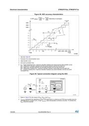
5.3.24 Embedded reference voltage
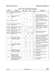
The parameters given in Table 72 are derived from tests performed under ambient
temperature and V
DD
supply voltage conditions summarized in Table 14.
5.3.25 DAC electrical characteristics
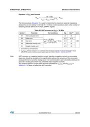
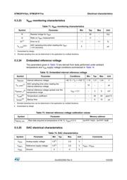
Table 71. V
BAT
monitoring characteristics
Symbol Parameter Min Typ Max Unit
R Resistor bridge for V
BAT
-50-KΩ
Q Ratio on V
BAT
measurement - 2 -
Er
(1)
Error on Q –1 - +1 %
T
S_vbat
(2)(2)
ADC sampling time when reading the V
BAT
1 mV accuracy
5--µs
1. Guaranteed by design.
2. Shortest sampling time can be determined in the application by multiple iterations.
Table 72. Embedded internal reference voltage
Symbol Parameter Conditions Min Typ
Max Unit
V
REFINT
Internal reference voltage –40 °C < T
A
< +105 °C 1.18 1.21 1.24 V
T
S_vrefint
(1)
ADC sampling time when reading the
internal reference voltage
-10--µs
V
RERINT_s
(2)
Internal reference voltage spread over the
temperature range
V
DD
= 3 V - 3 5 mV
T
Coeff
(2)
Temperature coefficient - - 30 50 ppm/°C
t
START
(2)
Startup time - - 6 10 µs
1. Shortest sampling time can be determined in the application by multiple iterations.
2. Guaranteed by design.
Table 73. Internal reference voltage calibration values
Symbol Parameter Memory address
V
REFIN_CAL
Raw data acquired at temperature of 30 °C, V
DDA
=3.3 V 0x1FFF 7A2A - 0x1FFF 7A2B
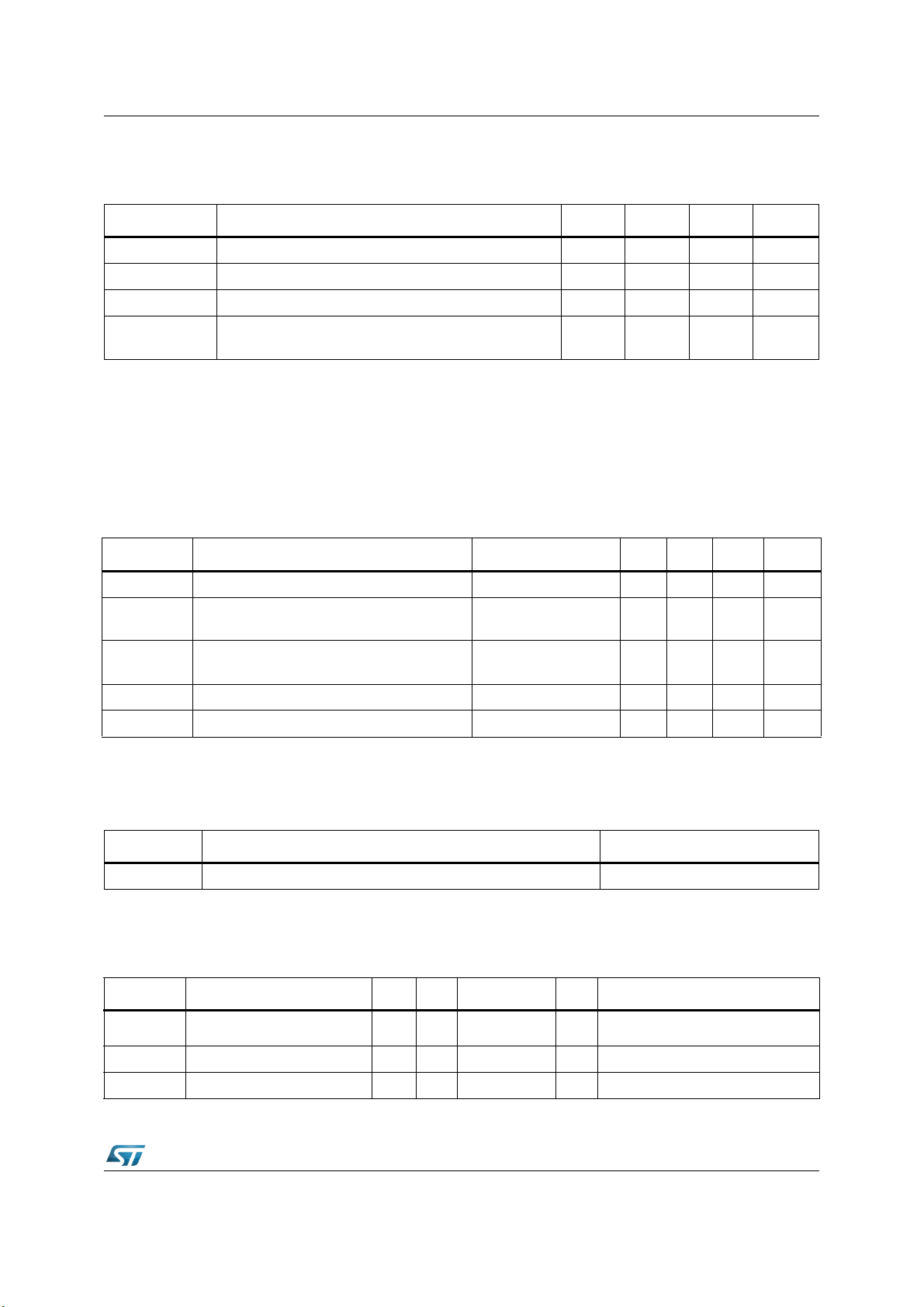
Table 74. DAC characteristics
Symbol Parameter Min Typ Max Unit Comments
V
DDA
Analog supply voltage 1.8
(1)
-3.6 V
V
REF+
Reference supply voltage 1.8
(1)
-3.6VV
REF+
≤ V
DDA
V
SSA
Ground 0 - 0 V
器件 Datasheet 文档搜索
AiEMA 数据库涵盖高达 72,405,303 个元件的数据手册,每天更新 5,000 多个 PDF 文件
