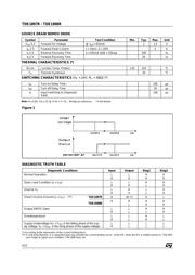
Datasheet 搜索 > FET驱动器 > ST Microelectronics(意法半导体) > TDE1897RFPT 数据手册 > TDE1897RFPT 数据手册 5/12 页
 器件3D模型
¥ 15.806
TDE1897RFPT 数据手册 - ST Microelectronics(意法半导体)
制造商:
ST Microelectronics(意法半导体)
分类:
FET驱动器
封装:
SOIC-20
描述:
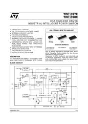
TDE1897系列 0.5 A 高边驱动器 工业智能电源开关 -DIP8
Pictures:
3D模型
符号图
焊盘图
引脚图
产品图
页面导航:
引脚图在P2Hot
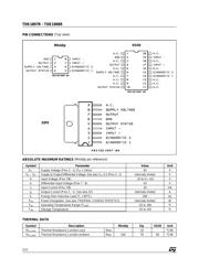
原理图在P1
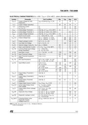
技术参数、封装参数在P2P12
电气规格在P3
导航目录
TDE1897RFPT数据手册
Page:
of 12 Go
若手册格式错乱,请下载阅览PDF原文件
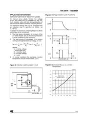
APPLICATION INFORMATION
DEMAGNETIZATION OF INDUCTIVE LOADS
An internal zener diode, limiting the voltage
across the Power MOS to between 45 and 55V
(V
cl
), provides safe and fast demagnetization of
inductive loads without external clamping devices.
The maximum energy that can be absorbed from
an inductive load is specified as 200mJ (at
T
j
= 85
°
C).
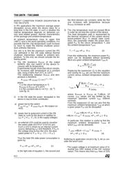
To define the maximum switching frequency three
points have to be considered:
1) The total power dissipation is the sum of the
On State Power and of the Demagnetization
Energy multiplied by the frequency.
2) The total energy W dissipated in the device
during a demagnetization cycle (figg. 2, 3) is:
W
=
V
cl
L
R
L
[
I
o
–
V
cl
– V
s
R
L
log
1
+
V
s
V
cl
– V
s
]
Where:
V
cl
= clamp voltage;
L = inductive load;
R
L
= resistive load;
Vs = supply voltage;
I
O
= I
LOAD
3) In normal conditions the operating Junction
temperature should remain below 125
°
C.
Figure 2:
Inductive Load Equivalent Circuit
Figure 3:
Demagnetization Cycle Waveforms
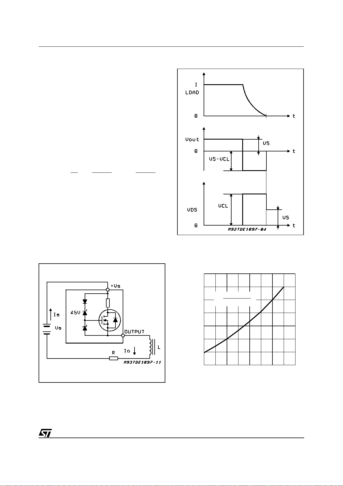
-25 0 25 50 75 100 125 Tj (˚C)
0.6
0.8
1.0
1.2
1.4
1.6
1.8
α
D93IN018
α=
RDSON (Tj)
RDSON (Tj=25˚C)
Figure 4:
Normalized R
DSON
vs. Junction
Temperature
TDE1897R - TDE1898R
5/12
器件 Datasheet 文档搜索
AiEMA 数据库涵盖高达 72,405,303 个元件的数据手册,每天更新 5,000 多个 PDF 文件
