Datasheet 搜索 > 接口芯片 > TI(德州仪器) > TFP410PAP 数据手册 > TFP410PAP 数据手册 4/29 页
 器件3D模型
¥ 16.366
TFP410PAP 数据手册 - TI(德州仪器)
制造商:
TI(德州仪器)
分类:
接口芯片
封装:
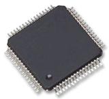
HTQFP-64
描述:
TEXAS INSTRUMENTS TFP410PAP 芯片, 发送器, 165MHz, PanelBus?
Pictures:
3D模型
符号图
焊盘图
引脚图
产品图
页面导航:
封装尺寸在P24
封装信息在P24P25
应用领域在P25P29
导航目录
TFP410PAP数据手册
Page:
of 29 Go
若手册格式错乱,请下载阅览PDF原文件
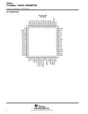
TFP410
TI PanelBus™ DIGITAL TRANSMITTER
SLDS145B − OCTOBER 2001 − REVISED MAY 2011
4
POST OFFICE BOX 655303 • DALLAS, TEXAS 75265
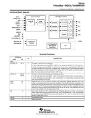
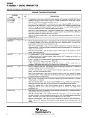
Terminal Functions (Continued)
TERMINAL
I/O
DESCRIPTION
NAME NO.
I/O
DESCRIPTION
CTL3/A3/DK3
CTL2/A2/DK2
CTL1/A1/DK1
6
7
8
I The operation of these three multifunction inputs depends on the settings of the ISEL (pin 13) and
DKEN (pin 35) inputs. All three inputs support 3.3-V CMOS signal levels and contain weak pulldown
resistors so that if left unconnected they default to all low.
When the I
2
C bus is disabled (ISEL = low) and the de-skew mode is disabled (DKEN = low), these three
inputs become the control inputs, CTL[3:1], which can be used to send additional information across
the DVI link during the blanking interval (DE = low). The CTL3 input is reserved for HDCP compliant DVI
TXs (TFP510) and the CTL[2:1] inputs are reserved for future use.
When the I
2
C bus is disabled (ISEL = low) and the de-skew mode is enabled (DKEN = high), these
three inputs become the de-skew inputs DK[3:1], used to adjust the setup and hold times of the pixel
data inputs DATA[23:0], relative to the clock input IDCK±.
When the I
2
C bus is enabled (ISEL = high), these three inputs become the 3 LSBs of the I
2
C slave
address, A[3:1].
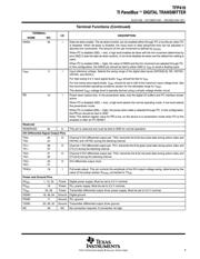
Configuration/Programming
MSEN/PO1 11 O Monitor sense/programmable output 1. The operation of this pin depends on whether the I
2
C interface
is enabled or disabled. This pin has an open-drain output and is only 3.3-V tolerant. An external 5-kΩ
pullup resistor connected to V
DD
is required on this pin.
When I
2
C is disabled (ISEL = low), a low level indicates a powered on receiver is detected at the
differential outputs. A high level indicates a powered on receiver is not detected. This function is only
valid in dc-coupled systems.
When I
2
C is enabled (ISEL = high), this output is programmable through the I
2
C interface (see the I
2
C
register descriptions section).
ISEL/RST 13 I I
2
C interface select/I
2
C RESET (active low, asynchronous)
If ISEL is high, then the I
2
C interface is active. Default values for the I
2
C registers can be found in the
I
2
C register descriptions section.
If ISEL is low, then I
2
C is disabled and the chip configuration is specified by the configuration pins
(BSEL, DSEL, EDGE, V
REF
) and state pins (PD, DKEN).
If ISEL is brought low and then back high, the I
2
C state machine is reset. The register values are
changed to their default values and are not preserved from before the reset.
BSEL/SCL 15 I Input bus select/I
2
C clock input. The operation of this pin depends on whether the I
2
C interface is
enabled or disabled. This pin is only 3.3-V tolerant.
When I
2
C is disabled (ISEL = low), a high level selects 24-bit input, single-edge input mode. A low level
selects 12-bit input, dual-edge input mode.
When I
2
C is enabled (ISEL = high), this pin functions as the I
2
C clock input (see the I
2
C register
descriptions section). In this configuration, this pin has an open-drain output that requires an external
5-kΩ pullup resistor connected to V
DD
.
DSEL/SDA 14 I/O DSEL/I
2
C data. The operation of this pin depends on whether the I
2
C interface is enabled or disabled.
This pin is only 3.3-V tolerant.
When I
2
C is disabled (ISEL = low), this pin is used with BSEL and V
REF
to select the single-ended or
differential input clock mode (see the universal graphics controller interface modes section).
When I
2
C is enabled (ISEL = high), this pin functions as the I
2
C bidirectional data line. In this
configuration, this pin has an open-drain output that requires an external 5-kΩ pullup resistor
connected to V
DD
.
EDGE/HTPLG 9 I Edge select/hot plug input. The operation of this pin depends on whether the I
2
C interface is enabled or
disabled. This input is 3.3-V tolerant only.
When I
2
C is disabled (ISEL = low), a high level selects the primary latch to occur on the rising edge of
the input clock IDCK+. A low level selects the primary latch to occur on the falling edge of the input clock
IDCK+. This is the case for both single-ended and differential input clock modes.
When I
2
C is enabled (ISEL = high), this pin is used to monitor the hot plug detect signal (see the DVI or
VESA™ P&D and DFP standards). When used for hot-plug detection, this pin requires a series 1-KΩ
resistor.
器件 Datasheet 文档搜索
AiEMA 数据库涵盖高达 72,405,303 个元件的数据手册,每天更新 5,000 多个 PDF 文件
