Datasheet 搜索 > 接口芯片 > TI(德州仪器) > TFP410PAP 数据手册 > TFP410PAP 数据手册 5/29 页
 器件3D模型
¥ 16.366
TFP410PAP 数据手册 - TI(德州仪器)
制造商:
TI(德州仪器)
分类:
接口芯片
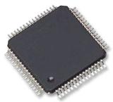
封装:
HTQFP-64
描述:
TEXAS INSTRUMENTS TFP410PAP 芯片, 发送器, 165MHz, PanelBus?
Pictures:
3D模型
符号图
焊盘图
引脚图
产品图
页面导航:
封装尺寸在P24
封装信息在P24P25
应用领域在P25P29
导航目录
TFP410PAP数据手册
Page:
of 29 Go
若手册格式错乱,请下载阅览PDF原文件
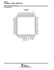
TFP410
TI PanelBus™ DIGITAL TRANSMITTER
SLDS145B − OCTOBER 2001 − REVISED MAY 2011
5
POST OFFICE BOX 655303 • DALLAS, TEXAS 75265
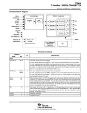
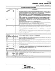
Terminal Functions (Continued)
TERMINAL
I/O
DESCRIPTION
NAME NO.
I/O
DESCRIPTION
DKEN 35 I Data de-skew enable. The de-skew function can be enabled either through I
2
C or by this pin when I
2
C
is disabled. When de-skew is enabled, the input clock to data setup/hold time can be adjusted in
discrete trim increments. The amount of trim per increment is defined by t
(STEP)
.
When I
2
C is disabled (ISEL = low), a high level enables de-skew with the trim increment determined by
pins DK[3:1] (see the data de-skew section). A low level disables de-skew and the default trim setting is
used.
When I
2
C is enabled (ISEL = high), the value of DKEN and the trim increment are selected through I
2
C.
In this configuration, the DKEN pin should be tied to either GND or V
DD
to avoid a floating input.
V
REF
3 I Input reference voltage. Selects the swing range of the digital data inputs (DATA[23:0], DE, HSYNC,
VSYNC, and IDCK±).
For high-swing 3.3-V input signal levels, V
REF
should be tied to V
DD
.
For low-swing input signal levels, V
REF
should be set to half of the maximum input voltage level. See
the recommended operating conditions section for the allowable range for V
REF
.
The desired V
REF
voltage level is typically derived using a simple voltage-divider circuit.
PD 10 I Power down (active low). In the powerdown state, only the digital I/O buffers and I
2
C interface remain
active.
When I
2
C is disabled (ISEL = low), a high level selects the normal operating mode. A low level selects
the powerdown mode.
When I
2
C is enabled (ISEL = high), the power-down state is selected through I
2
C. In this configuration,
the PD
pin should be tied to GND.
Note: The default register value for PD
is low, so the device is in powerdown mode when I
2
C is first
enabled or after an I
2
C RESET.
Reserved
RESERVED 34 In This pin is reserved and must be tied to GND for normal operation.
DVI Differential Signal Output Pins
TX0+
TX0−
25
24
O Channel 0 DVI differential output pair. TX0± transmits the 8-bit blue pixel data during active video and
HSYNC and VSYNC during the blanking interval.
TX1+
TX1−
28
27
O Channel 1 DVI differential output pair. TX1± transmits the 8-bit green pixel data during active video and
CTL[1] during the blanking interval.
TX2+
TX2−
31
30
O Channel 2 DVI differential output pair. TX2± transmits the 8-bit red pixel data during active video and
CTL[3:2] during the blanking interval.
TXC+
TXC−
22
21
O DVI differential output clock.
TFADJ 19 I Full-scale adjust. This pin controls the amplitude of the DVI output voltage swing, determined by the
value of the pullup resistor R
TFADJ
connected to TV
DD
.
Power and Ground Pins
DV
DD
1, 12, 33 Power Digital power supply. Must be set to 3.3 V nominal.
PV
DD
18 Power PLL power supply. Must be set to 3.3 V nominal.
TV
DD
23, 29 Power Transmitter differential output driver power supply. Must be set to 3.3 V nominal.
DGND 16, 48, 64 Ground Digital ground
PGND 17 Ground PLL ground
TGND 20, 26, 32 Ground Transmitter differential output driver ground
NC 49 NC No connection required. If connected, tie high.
器件 Datasheet 文档搜索
AiEMA 数据库涵盖高达 72,405,303 个元件的数据手册,每天更新 5,000 多个 PDF 文件
