Datasheet 搜索 > NXP(恩智浦) > TJA1051T118 数据手册 > TJA1051T118 数据手册 4/24 页

¥ 3.692
TJA1051T118 数据手册 - NXP(恩智浦)
制造商:
NXP(恩智浦)
Pictures:
3D模型
符号图
焊盘图
引脚图
产品图
页面导航:
导航目录
TJA1051T118数据手册
Page:
of 24 Go
若手册格式错乱,请下载阅览PDF原文件
TJA1051 All information provided in this document is subject to legal disclaimers. © NXP N.V. 2016. All rights reserved.
Product data sheet Rev. 8 — 12 July 2016 4 of 24
NXP Semiconductors
TJA1051
High-speed CAN transceiver
6. Pinning information
6.1 Pinning
6.2 Pin description
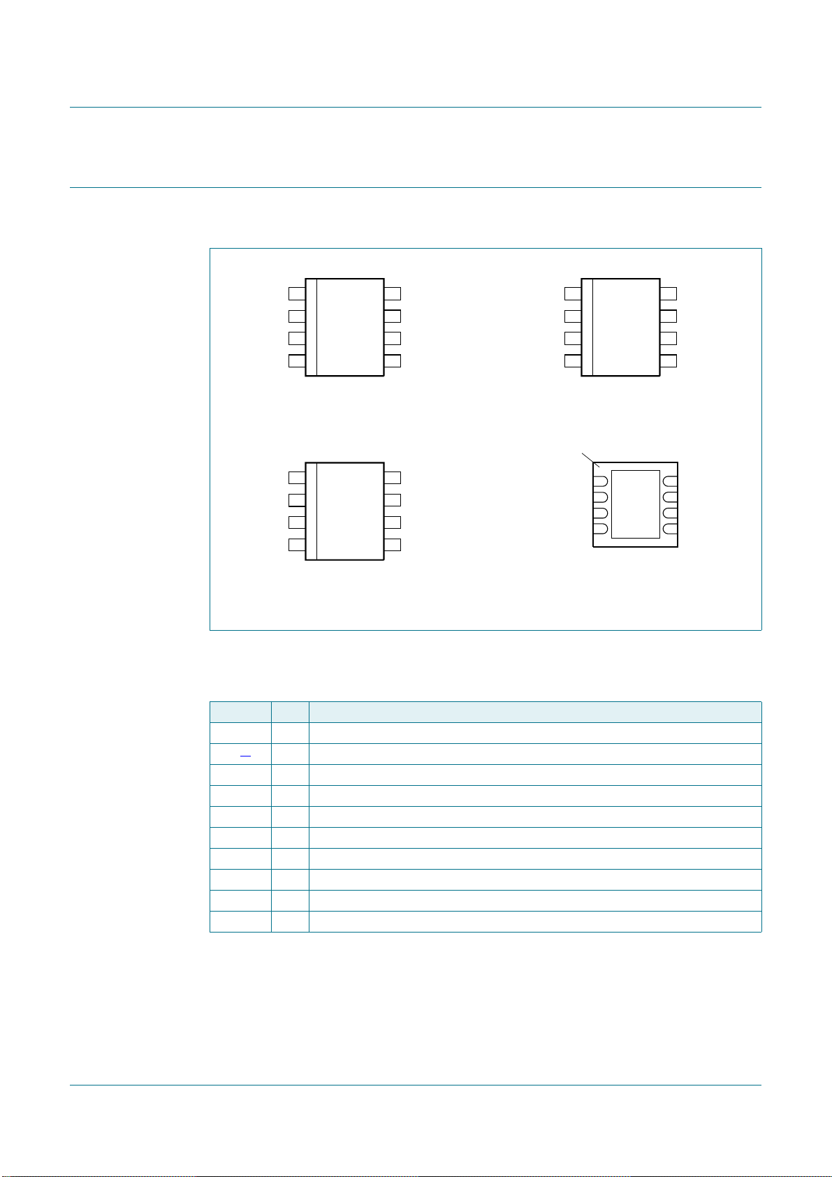
[1] HVSON8 package die supply ground is connected to both the GND pin and the exposed center pad. The
GND pin must be soldered to board ground. For enhanced thermal and electrical performance, it is
recommended that the exposed center pad also be soldered to board ground.
a. TJA1051T: SO8 b. TJA1051T/E: SO8
c. TJA1051T/3: SO8 d. TJA1051TK/3: HVSON8
Fig 2. Pin configuration diagrams
7;'
6
*1' &$1+
9
&&
&$1/
5;' QF
DDD
7-$7
7;'
6
*1' &$1+
9
&&
&$1/
5;'
(
1
DDD
7-$7(
7;'
6
*1' &$1+
9
&&
&$1/
5;'
9
,
2
DDD
7-$7
5;'
9
&&
*1'
7;'
9
,
2
&$1/
&$1+
6
DDD
7-$7.
WHUPLQDO
LQGH[DUHD
7UDQVSDUHQWWRSYLHZ
Table 3. Pin description
Symbol Pin Description
TXD 1 transmit data input
GND
[1]
2 ground
V
CC
3 supply voltage
RXD 4 receive data output; reads out data from the bus lines
n.c. 5 not connected; in TJA1051T version
EN 5 enable control input; TJA1051T/E only
V
IO
5 supply voltage for I/O level adapter; TJA1051T/3 and TJA1051TK/3 only
CANL 6 LOW-level CAN bus line
CANH 7 HIGH-level CAN bus line
S 8 Silent mode control input
器件 Datasheet 文档搜索
AiEMA 数据库涵盖高达 72,405,303 个元件的数据手册,每天更新 5,000 多个 PDF 文件
