Datasheet 搜索 > 负载控制器 > TI(德州仪器) > TPS22965DSGR 数据手册 > TPS22965DSGR 数据手册 4/28 页

¥ 0.617
TPS22965DSGR 数据手册 - TI(德州仪器)
制造商:
TI(德州仪器)
分类:
负载控制器
封装:
WSON-8
描述:
TEXAS INSTRUMENTS TPS22965DSGR 芯片, 功率负载开关, 5.7V, WSON-8 新
Pictures:
3D模型
符号图
焊盘图
引脚图
产品图
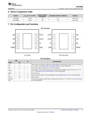
页面导航:
引脚图在P3Hot
典型应用电路图在P17
原理图在P1P14
封装尺寸在P21P23P24
焊盘布局在P19
标记信息在P21
封装信息在P20P21P22P23P24
技术参数、封装参数在P4
应用领域在P1P28
电气规格在P5P6P16
导航目录
TPS22965DSGR数据手册
Page:
of 28 Go
若手册格式错乱,请下载阅览PDF原文件
TPS22965
SLVSBJ0D –AUGUST 2012–REVISED JUNE 2015
www.ti.com
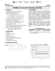
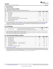
8 Specifications
8.1 Absolute Maximum Ratings
over operating free-air temperature range (unless otherwise noted)
(1) (2)
MIN MAX UNIT
V
IN
Input voltage –0.3 6 V
V
OUT
Output voltage –0.3 6 V
V
BIAS
Bias voltage –0.3 6 V
V
ON
On voltage –0.3 6 V
I
MAX
Maximum continuous switch current 6 A
I
PLS
Maximum pulsed switch current, pulse < 300 µs, 2% duty cycle 8 A
T
J
Maximum junction temperature 125 °C
T
stg
Storage temperature –65 150 °C
(1) Stresses beyond those listed under Absolute Maximum Ratings may cause permanent damage to the device. These are stress ratings
only, and functional operation of the device at these or any other conditions beyond those indicated under Recommended Operating
Conditions are not implied. Exposure to absolute–maximum–rated conditions for extended periods may affect device reliability.
(2) All voltage values are with respect to network ground pin.
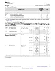
8.2 ESD Ratings
VALUE UNIT
Human-body model (HBM), per ANSI/ESDA/JEDEC JS-001
(1)
±2000
V
(ESD)
Electrostatic discharge V
Charged-device model (CDM), per JEDEC specification JESD22-C101
(2)
±1000
(1) JEDEC document JEP155 states that 500-V HBM allows safe manufacturing with a standard ESD control process. Manufacturing with
less than 500-V HBM is possible with the necessary precautions.
(2) JEDEC document JEP157 states that 250-V CDM allows safe manufacturing with a standard ESD control process. Manufacturing with
less than 250-V CDM is possible with the necessary precautions.
8.3 Recommended Operating Conditions
MIN MAX UNIT
V
IN
Input voltage range 0.8 V
BIAS
V
V
BIAS
Bias voltage range 2.5 5.7 V
V
ON
ON voltage range 0 5.7 V
V
OUT
Output voltage range V
IN
V
V
IH
High-level input voltage, ON V
BIAS
= 2.5 V to 5.7 V 1.1 5.7 V
V
IL
Low-level input voltage, ON V
BIAS
= 2.5 V to 5.7 V 0 0.5 V
C
IN
Input capacitor 1
(1)
µF
T
A
Operating free-air temperature range
(2)
–40 105 °C
(1) Refer to Application Information .
(2) In applications where high power dissipation and/or poor package thermal resistance is present, the maximum ambient temperature may
have to be derated. Maximum ambient temperature [T
A(max)
] is dependent on the maximum operating junction temperature [T
J(max)
], the
maximum power dissipation of the device in the application [P
D(max)
], and the junction-to-ambient thermal resistance of the part/package
in the application (θ
JA
), as given by the following equation: T
A (max)
= T
J(max)
– (θ
JA
× P
D(max)
)
4 Submit Documentation Feedback Copyright © 2012–2015, Texas Instruments Incorporated
Product Folder Links: TPS22965
器件 Datasheet 文档搜索
AiEMA 数据库涵盖高达 72,405,303 个元件的数据手册,每天更新 5,000 多个 PDF 文件
