Datasheet 搜索 > 稳压芯片 > TI(德州仪器) > TPS62130AQRGTRQ1 数据手册 > TPS62130AQRGTRQ1 数据手册 1/35 页
 器件3D模型
¥ 8.142
TPS62130AQRGTRQ1 数据手册 - TI(德州仪器)
制造商:
TI(德州仪器)
分类:
稳压芯片
封装:
VQFN-16
描述:
采用 3 × 3 QFN 封装的 TPS62130A-Q1 3V 至 17V 3A 汽车类降压转换器 16-VQFN -40 to 125
Pictures:
3D模型
符号图
焊盘图
引脚图
产品图
页面导航:
引脚图在P3Hot
典型应用电路图在P14P15
原理图在P1P9P10P14
封装尺寸在P28P31P33P34
焊盘布局在P29
标记信息在P3P31
封装信息在P27P31P32P33P34
技术参数、封装参数在P4
应用领域在P1P14P35
电气规格在P5P12
导航目录
TPS62130AQRGTRQ1数据手册
Page:
of 35 Go
若手册格式错乱,请下载阅览PDF原文件
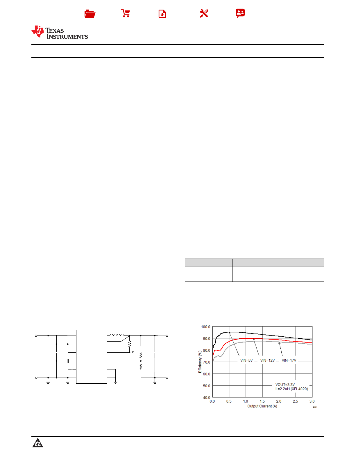
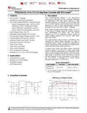
22uF
2.5V / 3A
10uF
(3 .. 17)V
3.3nF
TPS62130A-Q1
510k
240k
PVIN
AVIN
EN
SS/TR
DEF
LOG
SW
VOS
PG
FB
AGND
PGND
100k
0.1uF
1 / 2.2 µH
Product
Folder
Sample &
Buy
Technical
Documents
Tools &
Software
Support &
Community
TPS62130A-Q1
,
TPS62133A-Q1
SLVSCC2 –MAY 2014
TPS6213xA-Q1 3-V to 17-V 3-A Step-Down Converter with DCS-Control™
1 Features 3 Description
The TPS62130A-Q1 device is an easy-to-use
1
• DCS-Control™ Topology
synchronous step-down DC-DC converter optimized
• Qualified for Automotive Applications
for applications with high power density. A high
• AEC-Q100 Qualified With the Following Results:
switching frequency of typically 2.5 MHz allows the
use of small inductors and provides fast transient
– Device Temperature Grade: –40°C to 125°C
response as well as high output-voltage accuracy
Operating Junction Temperature Range
through the use of the DCS-Control™ topology.
– Device HBM ESD Classification Level H2
With a wide operating input-voltage range of 3 to 17
– Device CDM ESD Classification Level C4B
V, the device is ideally suited for systems powered
• Input Voltage Range: 3 to 17V
from intermediate bus power rails. The device
• Adjustable Output Voltage from 0.9 to 6V
supports up to 3-A continuous output current at
output voltages between 0.9 V and 6 V (with 100%
• Pin-Selectable Output Voltage (nominal, + 5%)
duty cycle mode).
• Programmable Soft Start and Tracking
The output-voltage startup ramp is controlled by the
• Seamless Power Save Mode Transition
soft-start pin, which allows operation as either a
• Quiescent Current of 17µA (typ.)
standalone power supply or in tracking configurations.
• Power Good Output
Power sequencing is also possible by configuring the
enable and open-drain power-good pins.
• 100% Duty Cycle Mode
• Short Circuit Protection
In power save mode, the device shows quiescent
current of about 17 μA from V
IN
. Power save mode
• Over Temperature Protection
which is entered automatically and seamlessly if the
• Available in a 3 × 3 mm, VQFN-16 Package
load is small, maintains high efficiency over the entire
load range. In shutdown mode, the device is turned
2 Applications
off and shutdown current consumption is less than 2
μA. The device is packaged in a 16-pin VQFN
• Automotive POL supply
package measuring 3 × 3 mm (RGT).
• Standard 12-V Rail Supplies
• Embedded Systems
Device Information
(1)
• LDO Replacement
PART NUMBER PACKAGE BODY SIZE (NOM)
TPS62130A-Q1
VQFN (16) 3.00 mm x 3.00 mm
TPS62133A-Q1
(1) For all available packages, see the orderable addendum at
the end of the datasheet.
4 Simplified Schematic
Efficiency vs Output Current
space
1
An IMPORTANT NOTICE at the end of this data sheet addresses availability, warranty, changes, use in safety-critical applications,
intellectual property matters and other important disclaimers. PRODUCTION DATA.
器件 Datasheet 文档搜索
AiEMA 数据库涵盖高达 72,405,303 个元件的数据手册,每天更新 5,000 多个 PDF 文件
