Datasheet 搜索 > DC/DC转换器 > TI(德州仪器) > TPS63020QDSJTQ1 数据手册 > TPS63020QDSJTQ1 数据手册 1/26 页

¥ 19.881
TPS63020QDSJTQ1 数据手册 - TI(德州仪器)
制造商:
TI(德州仪器)
分类:
DC/DC转换器
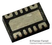
封装:
VSON EP-14
描述:
TEXAS INSTRUMENTS TPS63020QDSJTQ1 AEC-Q100 新
Pictures:
3D模型
符号图
焊盘图
引脚图
产品图
页面导航:
导航目录
TPS63020QDSJTQ1数据手册
Page:
of 26 Go
若手册格式错乱,请下载阅览PDF原文件
!"# $%$&'(
)
*+
,-)!)
.
,-)
)
*+
,-)!)
.
,-)
)
*+
,-)!)
.
,-)
)
*+
,-)!)
.
,-)
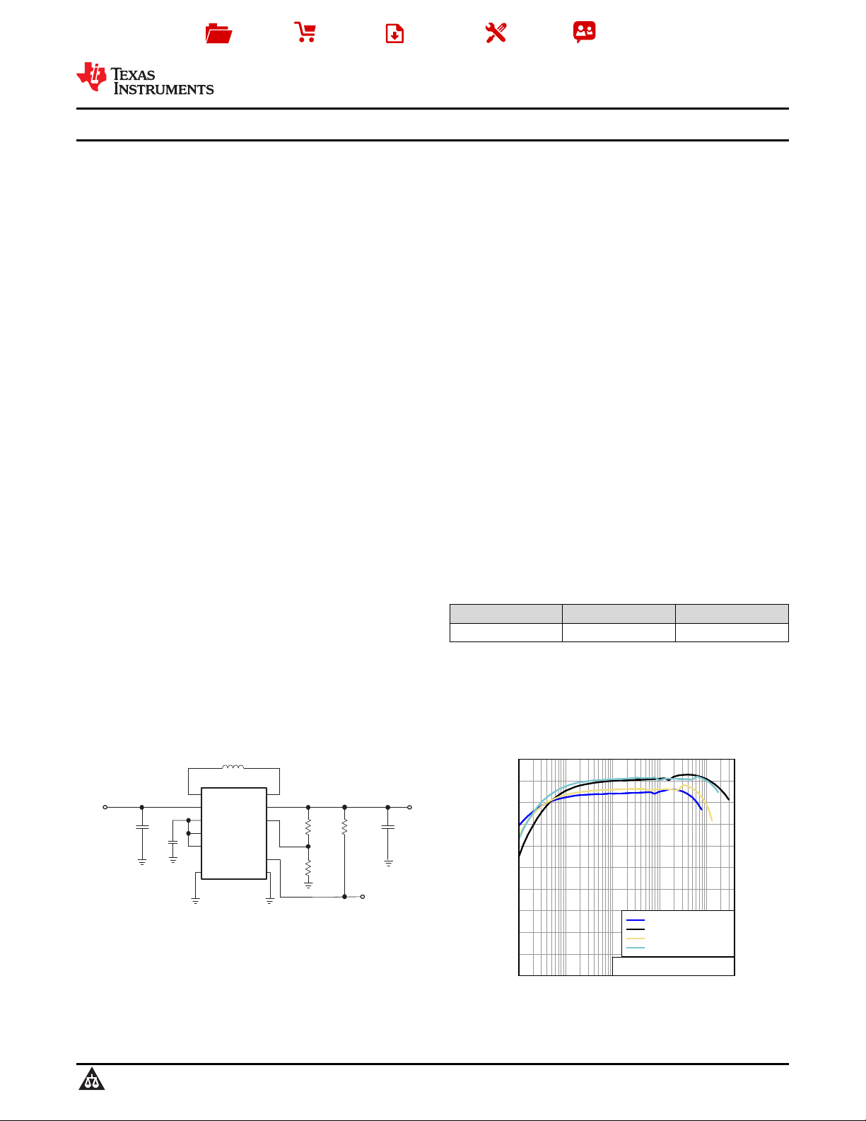
V
IN
L1
VIN
VINA
EN
PS/SYNC
GND
L2
VOUT
FB
PGND
L
1
1µH
C
2
C
3
2.5 V to
5.5V
V
OUT
3.3V
2A
TPS63020
PG
Power Good
Output
C
1
2X10µF
0.1µF
4X22µF
1MΩ
180kΩ
R
1
R
2
1MΩ
R
3
Product
Folder
Sample &
Buy
Technical
Documents
Tools &
Software
Support &
Community
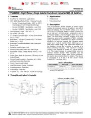
TPS63020-Q1
SLVSD52 –OCTOBER 2015
TPS63020-Q1 High Efficiency Single Inductor Buck-Boost Converter With 4-A Switches
1 Features 2 Applications
1
• Qualified for Automotive Applications
• Infotainment
• AEC-Q100 Qualified with the Following Results: • Telematics/eCall
– Device Temperature Grade: –40°C to 125°C
3 Description
Operating Junction Temperature Range
The TPS63020-Q1 device provides a power supply
– Device HBM ESD Classification Level H1B
solution for products powered by either a two-cell or
– Device CDM ESD Classification Level C4B
three-cell alkaline, NiCd or NiMH battery, or a one-
• Input Voltage Range: 1.8 V to 5.5 V
cell Li-Ion or Li-Polymer battery. Output currents can
go as high as 3 A while using a single-cell Li-Ion or
• Up to 96% Efficiency
Li-Polymer battery, and discharge it down to 2.5 V or
• 3 A Output Current at 3.3 V in Step Down Mode
lower. The buck-boost converter is based on a fixed
(V
IN
> 3.6 V)
frequency, pulse width modulation (PWM) controller
• More than 2 A Output Current at 3.3 V in Boost
using synchronous rectification to obtain maximum
Mode (V
IN
> 2.5 V)
efficiency. At low load currents, the converter enters
power save mode to maintain high efficiency over a
• Automatic Transition Between Step Down and
wide load current range. The power save mode can
Boost Mode
be disabled, forcing the converter to operate at a
• Dynamic Input Current Limit
fixed switching frequency. The maximum average
• Device Quiescent Current less than 50 μA
current in the switches is limited to a typical value of
4 A. The output voltage is programmable using an
• Adjustable Output Voltage Range from 1.2 V to
external resistor divider. The converter can be
5.5 V
disabled to minimize battery drain. During shutdown,
• Power Save Mode for Improved Efficiency at Low
the load is disconnected from the battery. The device
Output Power
is packaged in a 3 mm × 4 mm 14-pin VSON
PowerPAD™ package (DSJ).
• Forced Fixed Frequency Operation at 2.4 MHz
and Synchronization Possible
Device Information
(1)
• Smart Power Good Output
PART NUMBER PACKAGE BODY SIZE (NOM)
• Load Disconnect During Shutdown
TPS63020-Q1 VSON (14) 3.00 mm x 4.00 mm
• Overtemperature Protection
(1) For all available packages, see the orderable addendum at
• Overvoltage Protection
the end of the data sheet.
• Available in a 3-mm × 4-mm, VSON-14 Package
4 Typical Application Schematic
Efficiency vs Output Current
1
An IMPORTANT NOTICE at the end of this data sheet addresses availability, warranty, changes, use in safety-critical applications,
intellectual property matters and other important disclaimers. PRODUCTION DATA.
器件 Datasheet 文档搜索
AiEMA 数据库涵盖高达 72,405,303 个元件的数据手册,每天更新 5,000 多个 PDF 文件
