Datasheet 搜索 > 稳压芯片 > TI(德州仪器) > TPS63020DSJR 数据手册 > TPS63020DSJR 数据手册 1/29 页

¥ 2.993
TPS63020DSJR 数据手册 - TI(德州仪器)
制造商:
TI(德州仪器)
分类:
稳压芯片
封装:
VSON-14
描述:
TEXAS INSTRUMENTS TPS63020DSJR 直流-直流开关降压, 升压稳压器, 可调, 1.8V-5.5V输入, 1.2V-5.5V/4A输出, 2.4MHz, VSON-14 新
Pictures:
3D模型
符号图
焊盘图
引脚图
产品图
页面导航:
引脚图在P3Hot
典型应用电路图在P1P12
原理图在P1P7P8
封装尺寸在P22P24P25
标记信息在P22
封装信息在P21P22P23P24P25
技术参数、封装参数在P3
应用领域在P1P29
电气规格在P5P9
导航目录
TPS63020DSJR数据手册
Page:
of 29 Go
若手册格式错乱,请下载阅览PDF原文件
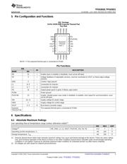
V
IN
L1
VIN
VINA
EN
PS/SYNC
GND
L2
VOUT
FB
PGND
L
1
1µH
C
2
C
3
2.5 V to
5.5V
V
OUT
3.3V
2A
TPS63020
PG
Power Good
Output
C
1
2X10µF
0.1µF
4X22µF
1MΩ
180kΩ
R
1
R
2
1MΩ
R
3
!"# $%$&'(
)
*+
,-)!)
.
,-)
)
*+
,-)!)
.
,-)
)
*+
,-)!)
.
,-)
)
*+
,-)!)
.
,-)
Product
Folder
Sample &
Buy
Technical
Documents
Tools &
Software
Support &
Community
TPS63020
,
TPS63021
SLVS916D –JULY 2010–REVISED OCTOBER 2015
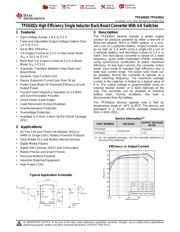
TPS6302x High Efficiency Single Inductor Buck-Boost Converter With 4-A Switches
1 Features 3 Description
The TPS6302x devices provide a power supply
1
• Input Voltage Range: 1.8 V to 5.5 V
solution for products powered by either a two-cell or
• Fixed and Adjustable Output Voltage Options from
three-cell alkaline, NiCd or NiMH battery, or a one-
1.2 V to 5.5 V
cell Li-ion or Li-polymer battery. Output currents can
• Up to 96% Efficiency
go as high as 3 A while using a single-cell Li-ion or
Li-polymer battery, and discharge it down to 2.5 V or
• 3-A Output Current at 3.3 V in Step Down Mode
lower. The buck-boost converter is based on a fixed
(V
IN
= 3.6 V to 5.5 V)
frequency, pulse width modulation (PWM) controller
• More than 2-A Output Current at 3.3 V in Boost
using synchronous rectification to obtain maximum
Mode (V
IN
> 2.5 V)
efficiency. At low load currents, the converter enters
• Automatic Transition Between Step Down and power save mode to maintain high efficiency over a
wide load current range. The power save mode can
Boost Mode
be disabled, forcing the converter to operate at a
• Dynamic Input Current Limit
fixed switching frequency. The maximum average
• Device Quiescent Current less than 50 μA
current in the switches is limited to a typical value of
• Power Save Mode for Improved Efficiency at Low
4 A. The output voltage is programmable using an
external resistor divider, or is fixed internally on the
Output Power
chip. The converter can be disabled to minimize
• Forced Fixed Frequency Operation at 2.4 MHz
battery drain. During shutdown, the load is
and Synchronization Possible
disconnected from the battery.
• Smart Power Good Output
The TPS6302x devices operate over a free air
• Load Disconnect During Shutdown
temperature range of –40°C to 85°C. The devices are
• Overtemperature Protection
packaged in a 14-pin VSON package measuring
3mm × 4mm (DSJ).
• Overvoltage Protection
• Available in a 3mm × 4mm 14-Pin VSON Package
Device Information
(1)
(DSJ)
OUTPUT VOLTAGE
PART NUMBER PACKAGE
DC/DC
2 Applications
TPS63020 Adjustable
VSON (14)
• All Two-Cell and Three-Cell Alkaline, NiCd or
TPS63021 3.3 V
NiMH or Single-Cell Li Battery Powered Products
(1) For all available packages, see the orderable addendum at
• Ultra Mobile PCs and Mobile Internet Devices
the end of the datasheet.
• Digital Media Players
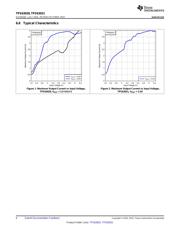
Efficiency vs Output Current
• Digital Still Cameras (DSC) and Camcorders
• Mobile Phones and Smart Phones
• Personal Medical Products
• Industrial Metering Equipment
• High Power LEDs
SPACE
Typical Application Schematic
1
An IMPORTANT NOTICE at the end of this data sheet addresses availability, warranty, changes, use in safety-critical applications,
intellectual property matters and other important disclaimers. PRODUCTION DATA.
器件 Datasheet 文档搜索
AiEMA 数据库涵盖高达 72,405,303 个元件的数据手册,每天更新 5,000 多个 PDF 文件
