Datasheet 搜索 > 稳压芯片 > TI(德州仪器) > TPS7A4701RGWR 数据手册 > TPS7A4701RGWR 数据手册 2/31 页
 器件3D模型
¥ 6.385
TPS7A4701RGWR 数据手册 - TI(德州仪器)
制造商:
TI(德州仪器)
分类:
稳压芯片
封装:
VQFN-20
描述:
TEXAS INSTRUMENTS TPS7A4701RGWR 芯片, 稳压器, LDO, 可调, 1A, 1.4V 至 20.5V, VQFN-20 新
Pictures:
3D模型
符号图
焊盘图
引脚图
产品图
页面导航:
引脚图在P4P5Hot
典型应用电路图在P16
原理图在P12
封装尺寸在P24P26P27
标记信息在P24
封装信息在P23P24P25P26P27
技术参数、封装参数在P5
应用领域在P1P31
电气规格在P7P17

导航目录
TPS7A4701RGWR数据手册
Page:
of 31 Go
若手册格式错乱,请下载阅览PDF原文件

TPS7A4700
,
TPS7A4701
SBVS204F –JUNE 2012–REVISED SEPTEMBER 2014
www.ti.com
Table of Contents
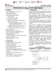
1 Features.................................................................. 1 8 Application and Implementation ........................ 16
8.1 Application Information............................................ 16
2 Applications ........................................................... 1
8.2 Typical Application ................................................. 16
3 Description ............................................................. 1
9 Power Supply Recommendations...................... 20
4 Revision History..................................................... 2
9.1 Power Dissipation (PD)........................................... 20
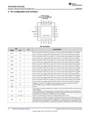
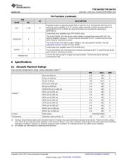
5 Pin Configuration and Functions......................... 4
10 Layout................................................................... 21
6 Specifications......................................................... 5
10.1 Layout Guidelines ................................................. 21
6.1 Absolute Maximum Ratings ...................................... 5
10.2 Layout Example .................................................... 21
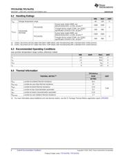
6.2 Handling Ratings....................................................... 6
10.3 Thermal Protection................................................ 22
6.3 Recommended Operating Conditions....................... 6
10.4 Estimating Junction Temperature ......................... 22
6.4 Thermal Information.................................................. 6
11 Device and Documentation Support................. 23
6.5 Electrical Characteristics........................................... 7
11.1 Documentation Support ........................................ 23
6.6 Typical Characteristics.............................................. 8
11.2 Related Links ........................................................ 23
7 Detailed Description............................................ 12
11.3 Trademarks........................................................... 23
7.1 Overview ................................................................. 12
11.4 Electrostatic Discharge Caution............................ 23
7.2 Functional Block Diagram....................................... 12
11.5 Glossary................................................................ 23
7.3 Feature Description................................................. 12
12 Mechanical, Packaging, and Orderable
7.4 Device Functional Modes........................................ 13
Information........................................................... 23
7.5 Programming........................................................... 13
4 Revision History
NOTE: Page numbers for previous revisions may differ from page numbers in the current version.
Changes from Revision E (January 2014) to Revision F Page
• Added Handling Rating table, Feature Description section, Device Functional Modes, Application and
Implementation section, Power Supply Recommendations section, Layout section, Device and Documentation
Support section, and Mechanical, Packaging, and Orderable Information section ............................................................... 1
• Reworded ninth bullet in Features list .................................................................................................................................... 1
• Changed polarity of op amp shown on right side of the functional block diagram .............................................................. 12
• Reworded second paragraph in Soft-Start And Inrush Current section .............................................................................. 13
• Revised Capacitor Recommendations section..................................................................................................................... 16
• Changed paragraph 2 of Dropout Voltage (V
DO
) section for clarity ..................................................................................... 17
• Revised paragraph 1 of Startup section .............................................................................................................................. 17
• Rewrote paragraph 1 of Power-Supply Rejection Ratio (PSRR) section to eliminate confusion ........................................ 18
• Changed paragraph 1 of Power Supply Recommendations section ................................................................................... 20
• Changed paragraph 1 and paragraph 4 of Power Dissipation (P
D
) section......................................................................... 20
• Revised paragraph 2 of Layout Guidelines section ............................................................................................................. 21
• Changed second paragraph of Thermal Protection section ................................................................................................ 22
Changes from Revision D (December 2013) to Revision E Page
• Changed Output Voltage Noise value from 4.17 µV to 4 µV in three instances on front page .............................................. 1
• Changed 2nd and 3rd paragraphs of Description section...................................................................................................... 1
• Added " Thermal Pad" to pin configuration drawing................................................................................................................ 4
• Changed EN pin description................................................................................................................................................... 4
• Changed SENSE/FB pin to be for TPS7A4701 only.............................................................................................................. 5
• Added new row to Pin Descriptions table for SENSE pin (for TPS7A4700 only)................................................................... 5
• Added new row to Pin Descriptions table for thermal pad ..................................................................................................... 5
• Added V
REF
parameter............................................................................................................................................................ 7
2 Submit Documentation Feedback Copyright © 2012–2014, Texas Instruments Incorporated
Product Folder Links: TPS7A4700 TPS7A4701
器件 Datasheet 文档搜索
AiEMA 数据库涵盖高达 72,405,303 个元件的数据手册,每天更新 5,000 多个 PDF 文件
