Datasheet 搜索 > 稳压芯片 > TI(德州仪器) > TPS7A4701RGWR 数据手册 > TPS7A4701RGWR 数据手册 5/31 页
 器件3D模型
¥ 6.385
TPS7A4701RGWR 数据手册 - TI(德州仪器)
制造商:
TI(德州仪器)
分类:
稳压芯片
封装:
VQFN-20
描述:
TEXAS INSTRUMENTS TPS7A4701RGWR 芯片, 稳压器, LDO, 可调, 1A, 1.4V 至 20.5V, VQFN-20 新
Pictures:
3D模型
符号图
焊盘图
引脚图
产品图
页面导航:
引脚图在P4P5Hot
典型应用电路图在P16
原理图在P12
封装尺寸在P24P26P27
标记信息在P24
封装信息在P23P24P25P26P27
技术参数、封装参数在P5
应用领域在P1P31
电气规格在P7P17

导航目录
TPS7A4701RGWR数据手册
Page:
of 31 Go
若手册格式错乱,请下载阅览PDF原文件
TPS7A4700
,
TPS7A4701
www.ti.com
SBVS204F –JUNE 2012–REVISED SEPTEMBER 2014
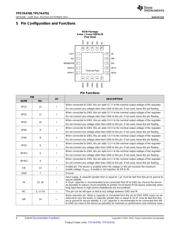
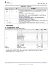
Pin Functions (continued)
PIN
I/O DESCRIPTION
NAME NO.
Regulator output. A capacitor greater than or equal to 10 µF must be tied from this pin to
ground to assure stability. A 47-µF ceramic output capacitor is highly recommended to be
OUT 1, 20 O
connected from OUT to GND (as close to the device as possible) to maximize ac
performance.
Control-loop error amplifier input (TPS7A4701 only).
This is the SENSE pin if the device output voltage is programmed using ANY-OUT (no
external feedback resistors). This pin must be connected to OUT. Connect this pin to the
SENSE/FB 3 I
point of load to maximize accuracy.
This is the FB pin if the device output voltage is set using external resistors. See the
Adjustable Operation section for more details.
Control-loop error amplifier input (TPS7A4700 only).
SENSE 3 I
This is the SENSE pin of the device and must be connected to OUT. Connect this pin to the
point of load to maximize accuracy.
Connect the thermal pad to a large-area ground plane. The thermal pad is internally
Thermal Pad —
connected to GND.
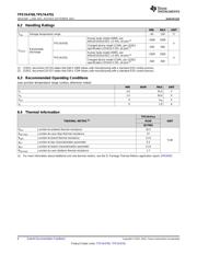
6 Specifications
6.1 Absolute Maximum Ratings
Over junction temperature range, unless otherwise noted.
(1)
MIN MAX UNIT
IN pin to GND pin –0.4 +36 V
EN pin to GND pin –0.4 +36 V
EN pin to IN pin –36 +0.4 V
OUT pin to GND pin –0.4 +36 V
NR pin to GND pin –0.4 +36 V
SENSE/FB pin to GND pin –0.4 +36 V
0P1V pin to GND pin –0.4 +36 V
Voltage
(2)
0P2V pin to GND pin –0.4 +36 V
0P4V pin to GND pin –0.4 +36 V
0P8V pin to GND pin –0.4 +36 V
1P6V pin to GND pin –0.4 +36 V
3P2V pin to GND pin –0.4 +36 V
6P4V1 pin to GND pin –0.4 +36 V
6P4V2 pin to GND pin –0.4 +36 V
Current Peak output Internally limited
Temperature Operating virtual junction, T
J
–40 125 °C
(1) Stresses beyond those listed under Absolute Maximum Ratings may cause permanent damage to the device. These are stress ratings
only, which do not imply functional operation of the device at these or any other conditions beyond those indicated under Recommended
Operating Conditions. Exposure to absolute-maximum-rated conditions for extended periods may affect device reliability..
(2) All voltages are with respect to network ground terminal.
Copyright © 2012–2014, Texas Instruments Incorporated Submit Documentation Feedback 5
Product Folder Links: TPS7A4700 TPS7A4701
器件 Datasheet 文档搜索
AiEMA 数据库涵盖高达 72,405,303 个元件的数据手册,每天更新 5,000 多个 PDF 文件
