Datasheet 搜索 > 接口芯片 > TI(德州仪器) > TRS232ECDR 数据手册 > TRS232ECDR 数据手册 5/10 页
 器件3D模型
¥ 7.529
TRS232ECDR 数据手册 - TI(德州仪器)
制造商:
TI(德州仪器)
分类:
接口芯片
封装:
SOIC-16
描述:
TEXAS INSTRUMENTS TRS232ECDR 线路接收器, RS232, 2驱动器, 4.5V-5.5电源, SOIC-16
Pictures:
3D模型
符号图
焊盘图
引脚图
产品图
页面导航:
引脚图在P2Hot
导航目录
TRS232ECDR数据手册
Page:
of 10 Go
若手册格式错乱,请下载阅览PDF原文件
5
impedance, V
CC
= 4.5V, and maximum allowable operating
temperature. The transmitters have an internally limited output
slew rate which is less than 30V/µs. The outputs are short
circuit protected and can be shorted to ground indefinitely. The
powered down output impedance is a minimum of 300Ω with
±2V applied to the outputs and V
CC
= 0V.
Receivers
The receiver inputs accept up to ±30V while presenting the
required 3kΩ to 7kΩ input impedance even if the power is off
(V
CC
= 0V). The receivers have a typical input threshold of 1.3V
which is within the ±3V limits, known as the transition region, of
the RS-232 specifications. The receiver output is 0V to V
CC
.
The output will be low whenever the input is greater than 2.4V
and high whenever the input is floating or driven between +0.8V
and -30V. The receivers feature 0.5V hysteresis (except during
shutdown) to improve noise rejection.
Application Information
The HIN232A may be used for all RS-232 data terminal and
communication links. It is particularly useful in applications
where ±12V power supplies are not available for
conventional RS-232 interface circuits. The applications
presented represent typical interface configurations.
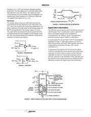
A simple duplex RS-232 port with CTS/RTS handshaking is
illustrated in Figure 7. Fixed output signals such as DTR
(data terminal ready) and DSRS (data signaling rate select)
is generated by driving them through a 5kΩ resistor
connected to V+.
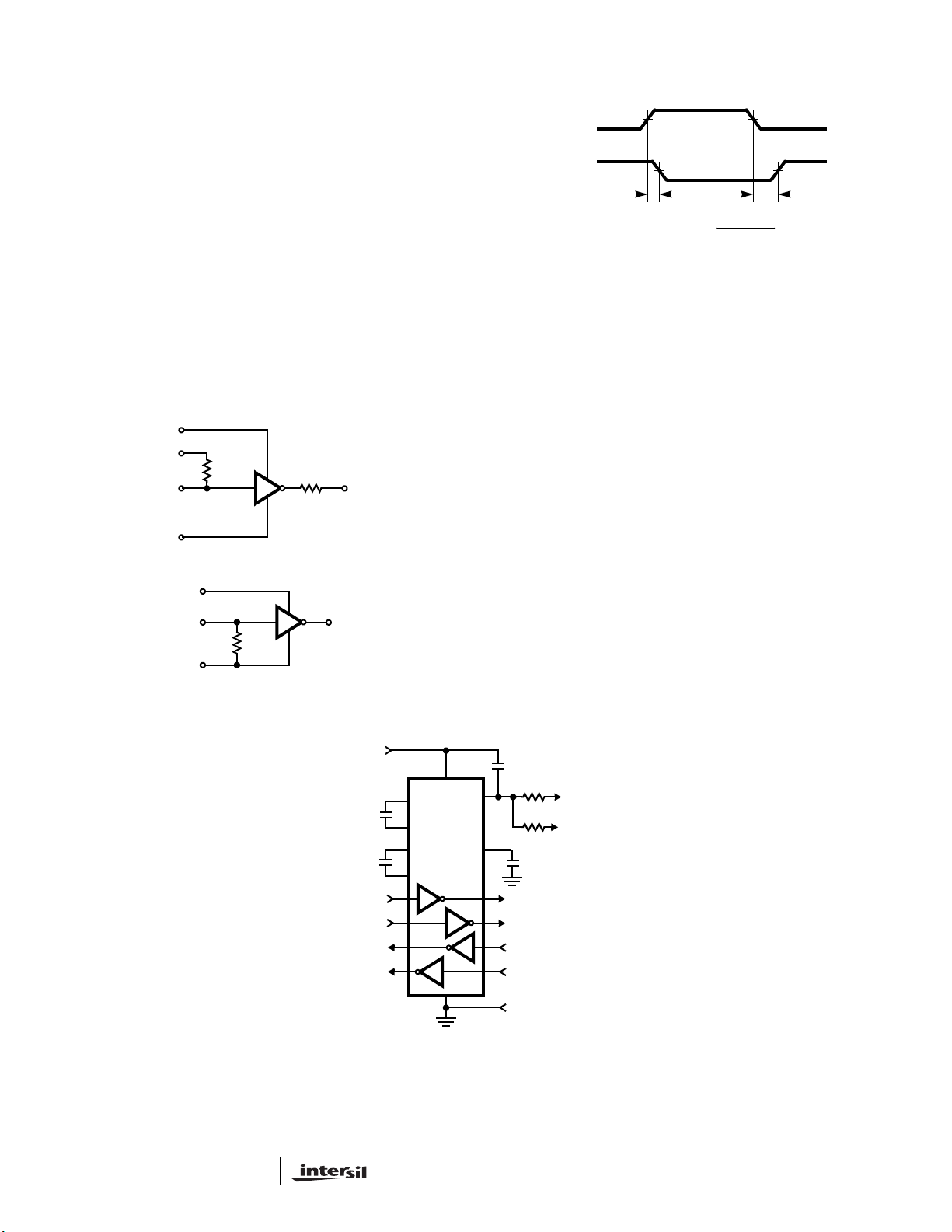
In applications requiring four RS-232 inputs and outputs
(Figure 8), note that each circuit requires two charge pump
capacitors (C1 and C2) but can share common reservoir
capacitors (C3 and C4). The benefit of sharing common
reservoir capacitors is the elimination of two capacitors and
the reduction of the charge pump source impedance which
effectively increases the output swing of the transmitters.
T
OUT
V- < V
TOUT
< V+
300Ω
400kΩ
T
XIN
GND < T
XIN
< V
CC
V-
V+
V
CC
FIGURE 4. TRANSMITTER
R
OUT
GND < V
ROUT
< V
CC
5kΩ
R
XIN
-30V < R
XIN
< +30V
GND
V
CC
FIGURE 5. RECEIVER
T
IN
V
OH
V
OL
t
PLH
t
PHL
AVERAGE PROPAGATION DELAY =
t
PHL +
t
PLH
2
OR
R
IN
T
OUT
OR
R
OUT
FIGURE 6. PROPAGATION DELAY DEFINITION
-
+
-
+
-
+
CTR (20) DATA
TERMINAL READY
DSRS (24) DATA
SIGNALING RATE
RS-232
INPUTS AND OUTPUTS
TD (2) TRANSMIT DATA
RTS (4) REQUEST TO SEND
RD (3) RECEIVE DATA
CTS (5) CLEAR TO SEND
SIGNAL GROUND (7)15
8
13
7
14
16
-
+
6
R2
R1
T2
T1
9
12
10
11
4
5
3
1
HIN232A
C1
0.1µF
C2
0.1µF
TD
RTS
RD
CTS
SELECT
+5V
INPUTS
OUTPUTS
TTL/CMOS
FIGURE 7. SIMPLE DUPLEX RS-232 PORT WITH CTS/RTS HANDSHAKING
HIN232A
器件 Datasheet 文档搜索
AiEMA 数据库涵盖高达 72,405,303 个元件的数据手册,每天更新 5,000 多个 PDF 文件
