Datasheet 搜索 > 接口芯片 > TI(德州仪器) > TRSF3223ECPWR 数据手册 > TRSF3223ECPWR 数据手册 4/29 页
 器件3D模型
¥ 38.441
TRSF3223ECPWR 数据手册 - TI(德州仪器)
制造商:
TI(德州仪器)
分类:
接口芯片
封装:
TSSOP-20
描述:
3V至5.5V多通道RS - 232线路驱动器/接收器,具有± 15 kV ESD保护 3-V TO 5.5-V MULTICHANNEL RS-232 LINE DRIVER/RECEIVER WITH ±15-kV ESD PROTECTION
Pictures:
3D模型
符号图
焊盘图
引脚图
产品图
页面导航:
典型应用电路图在P3
封装尺寸在P2P13P15P16P25
焊盘布局在P26
型号编码规则在P1P2
标记信息在P2P13P14
封装信息在P2P13P14P15P16
技术参数、封装参数在P4
应用领域在P1P29
电气规格在P4P5P6P7
导航目录
TRSF3223ECPWR数据手册
Page:
of 29 Go
若手册格式错乱,请下载阅览PDF原文件
TRSF3223E
SLLS824A –AUGUST 2007–REVISED SEPTEMBER 2011
www.ti.com
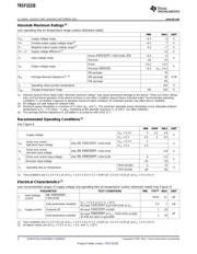
Absolute Maximum Ratings
(1)
over operating free-air temperature range (unless otherwise noted)
MIN MAX UNIT
V
CC
Supply voltage range –0.3 6 V
V+ Positive-output supply voltage range
(2)
–0.3 7 V
V– Negative-output supply voltage range
(2)
0.3 –7 V
V+ – V– Supply voltage difference
(2)
13 V
Driver (FORCEOFF, FORCEON, EN) –0.3 6
V
I
Input voltage range V
Receiver –25 25
Driver –13.2 13.2
V
O
Output voltage range V
Receiver (INVALID) –0.3 V
CC
+ 0.3
DB package 70
θ
JA
Package thermal impedance
(3) (4)
DW package 58 °C/W
PW package 83
T
J
Operating virtual junction temperature 150 °C
T
stg
Storage temperature range –65 150 °C
(1) Stresses beyond those listed under "absolute maximum ratings" may cause permanent damage to the device. These are stress ratings
only, and functional operation of the device at these or any other conditions beyond those indicated under "recommended operating
conditions" is not implied. Exposure to absolute-maximum-rated conditions for extended periods may affect device reliability.
(2) All voltages are with respect to network GND.
(3) Maximum power dissipation is a function of T
J
(max), θ
JA
, and T
A
. The maximum allowable power dissipation at any allowable ambient
temperature is P
D
= (T
J
(max) – T
A
)/θ
JA
. Operating at the absolute maximum T
J
of 150°C can affect reliability.
(4) The package thermal impedance is calculated in accordance with JESD 51-7.
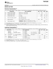
Recommended Operating Conditions
(1)
See Figure 6
MIN NOM MAX UNIT
V
CC
= 3.3 V 3 3.3 3.6
Supply voltage V
V
CC
= 5 V 4.5 5 5.5
V
CC
= 3.3 V 2
Driver and control
V
IH
DIN, EN, FORCEOFF, FORCEON V
high-level input voltage
V
CC
= 5 V 2.4
Driver and control
V
IL
DIN, EN, FORCEOFF, FORCEON 0.8 V
low-level input voltage
Driver and control input voltage DIN, EN, FORCEOFF, FORCEON 0 5.5
V
I
V
Receiver input voltage –25 25
TRSF3223EC 0 70
T
A
Operating free-air temperature °C
TRSF3223EI –40 85
(1) Test conditions are C1–C4 = 0.1 μF at V
CC
= 3.3 V ± 0.3 V; C1 = 0.047 μF, C2–C4 = 0.33 μF at V
CC
= 5 V ± 0.5 V.
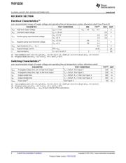
Electrical Characteristics
(1)
over recommended ranges of supply voltage and operating free-air temperature (unless otherwise noted) (see Figure 5)
PARAMETER TEST CONDITIONS MIN TYP
(2)
MAX UNIT
Input leakage EN, FORCEOFF,
I
I
±0.01 ±1 μA
current FORCEON
V
CC
= 3.3 V or 5 V, T
A
= 25°C,
Auto-powerdown disabled 0.3 1 mA
No load, FORCEOFF and FORCEON at V
CC
I
CC
Supply current Powered off No load, FORCEOFF at GND 1 10
μA
No load, FORCEOFF at V
CC
, FORCEON at GND,
Auto-powerdown enabled 1 10
All RIN are open or grounded
(1) Test conditions are C1–C4 = 0.1 μF at V
CC
= 3.3 V ± 0.3 V; C1 = 0.047 μF, C2–C4 = 0.33 μF at V
CC
= 5 V ± 0.5 V.
(2) All typical values are at V
CC
= 3.3 V or V
CC
= 5 V, and T
A
= 25°C.
4 Submit Documentation Feedback Copyright © 2007–2011, Texas Instruments Incorporated
Product Folder Link(s): TRSF3223E
器件 Datasheet 文档搜索
AiEMA 数据库涵盖高达 72,405,303 个元件的数据手册,每天更新 5,000 多个 PDF 文件
