Datasheet 搜索 > 逻辑芯片 > TI(德州仪器) > TS3DV520RHUR 数据手册 > TS3DV520RHUR 数据手册 4/20 页
 器件3D模型
¥ 0.61
TS3DV520RHUR 数据手册 - TI(德州仪器)
制造商:
TI(德州仪器)
分类:
逻辑芯片
封装:
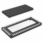
WQFN-56
描述:
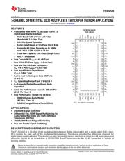
5通道差分10:20多路器开关用于DVI / HDMI应用 5-CHANNEL DIFFERENTIAL 10:20 MULTIPLEXER SWITCH FOR DVI/HDMI APPLICATIONS
Pictures:
3D模型
符号图
焊盘图
引脚图
产品图
页面导航:
引脚图在P2Hot
典型应用电路图在P3
封装尺寸在P2P13P15P16
型号编码规则在P1P2
标记信息在P2P13
封装信息在P2P13P14P15P16
技术参数、封装参数在P4
应用领域在P1P20
电气规格在P5
导航目录
TS3DV520RHUR数据手册
Page:
of 20 Go
若手册格式错乱,请下载阅览PDF原文件
TS3DV520
SCDS197D –DECEMBER 2005–REVISED OCTOBER 2009
www.ti.com
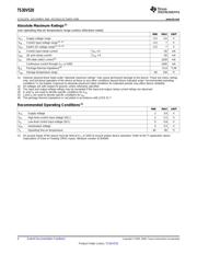
Absolute Maximum Ratings
(1)
over operating free-air temperature range (unless otherwise noted)
MIN MAX UNIT
V
CC
Supply voltage range –0.5 4.6 V
V
IN
Control input voltage range
(2) (3)
–0.5 7 V
V
I/O
Switch I/O voltage range
(2) (3) (4)
–0.5 7 V
I
IK
Control input clamp current V
IN
< 0 –50 mA
I
I/OK
I/O port clamp current V
I/O
< 0 –50 mA
I
I/O
ON-state switch current
(5)
±128 mA
Continuous current through V
CC
or GND ±100 mA
θ
JA
Package thermal impedance
(6)
31.8 °C/W
T
stg
Storage temperature range –65 150 °C
(1) Stresses beyond those listed under "absolute maximum ratings" may cause permanent damage to the device. These are stress ratings
only, and functional operation of the device at these or any other conditions beyond those indicated under "recommended operating
conditions" is not implied. Exposure to absolute-maximum-rated conditions for extended periods may affect device reliability.
(2) All voltages are with respect to ground, unless otherwise specified.
(3) The input and output voltage ratings may be exceeded if the input and output clamp-current ratings are observed.
(4) V
I
and V
O
are used to denote specific conditions for V
I/O
.
(5) I
I
and I
O
are used to denote specific conditions for I
I/O
.
(6) The package thermal impedance is calculated in accordance with JESD 51-7.
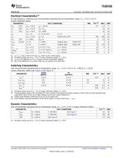
Recommended Operating Conditions
(1)
MIN MAX UNIT
V
CC
Supply voltage 3 3.6 V
V
IH
High-level control input voltage (SEL) 2 5.5 V
V
IL
Low-level control input voltage (SEL) 0 0.8 V
V
I/O
Input/output voltage 0 5.5 V
T
A
Operating free-air temperature –40 85 °C
(1) All unused inputs of the device must be held at V
CC
or GND to ensure proper device operation. Refer to the TI application report,
Implications of Slow or Floating CMOS Inputs, literature number SCBA004.
4 Submit Documentation Feedback Copyright © 2005–2009, Texas Instruments Incorporated
Product Folder Link(s): TS3DV520
器件 Datasheet 文档搜索
AiEMA 数据库涵盖高达 72,405,303 个元件的数据手册,每天更新 5,000 多个 PDF 文件
