Datasheet 搜索 > 逻辑芯片 > TI(德州仪器) > TS3DV520RHUR 数据手册 > TS3DV520RHUR 数据手册 5/20 页
 器件3D模型
¥ 0.61
TS3DV520RHUR 数据手册 - TI(德州仪器)
制造商:
TI(德州仪器)
分类:
逻辑芯片
封装:
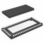
WQFN-56
描述:
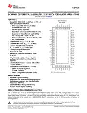
5通道差分10:20多路器开关用于DVI / HDMI应用 5-CHANNEL DIFFERENTIAL 10:20 MULTIPLEXER SWITCH FOR DVI/HDMI APPLICATIONS
Pictures:
3D模型
符号图
焊盘图
引脚图
产品图
页面导航:
引脚图在P2Hot
典型应用电路图在P3
封装尺寸在P2P13P15P16
型号编码规则在P1P2
标记信息在P2P13
封装信息在P2P13P14P15P16
技术参数、封装参数在P4
应用领域在P1P20
电气规格在P5
导航目录
TS3DV520RHUR数据手册
Page:
of 20 Go
若手册格式错乱,请下载阅览PDF原文件

TS3DV520
www.ti.com
SCDS197D –DECEMBER 2005–REVISED OCTOBER 2009
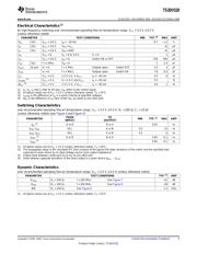
Electrical Characteristics
(1)
for high-frequency switching over recommended operating free-air temperature range, V
CC
= 3.3 V ± 0.3 V
(unless otherwise noted)
PARAMETER TEST CONDITIONS MIN TYP
(2)
MAX UNIT
V
IK
SEL V
CC
= 3.6 V, I
IN
= –18 mA –0.7 –1.2 V
I
IH
SEL V
CC
= 3.6 V, V
IN
= V
CC
±1 μA
I
IL
SEL V
CC
= 3.6 V, V
IN
= GND ±1 μA
I
off
V
CC
= 0, V
O
= 0 to 3.6 V, V
I
= 0 1 μA
I
CC
V
CC
= 3.6 V, I
I/O
= 0, Switch ON or OFF 250 500 μA
C
IN
SEL f = 1 MHz, V
IN
= 0 2 2.5 pF
C
OFF
B port V
I
= 0, f = 1 MHz, Outputs open, Switch OFF 2.5 3 pF
C
ON
V
I
= 0, f = 1 MHz, Outputs open, Switch ON 7.8 8.5 pF
r
on
V
CC
= 3 V, 1.5 V ≤ V
I
≤ V
CC
, I
O
= –40 mA 3.5 6 Ω
r
on(flat)
(3)
V
CC
= 3 V, V
I
= 1.5 V and V
CC
, I
O
= –40 mA 0.5 Ω
Δr
on
(4)
V
CC
= 3 V, 1.5 V ≤ V
I
≤ V
CC
, I
O
= –40 mA 0.4 1 Ω
(1) V
I
, V
O
, I
I
, and I
O
refer to I/O pins. V
IN
refers to the control inputs.
(2) All typical values are at V
CC
= 3.3 V (unless otherwise noted), T
A
= 25°C.
(3) r
on(flat)
is the difference of r
on
in a given channel at specified voltages.
(4) Δr
on
is the difference of r
on
from center (A
4
, A
5
) ports to any other port.
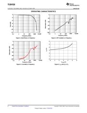
Switching Characteristics
over recommended operating free-air temperature range, V
CC
= 3.3 V ± 0.3 V, R
L
= 200 Ω, C
L
= 10 pF
(unless otherwise noted) (see Figure 4 and Figure 5)
FROM TO
PARAMETER MIN TYP
(1)
MAX UNIT
(INPUT) (OUTPUT)
t
pd
(2)
A or B B or A 0.25 ns
t
PZH
, t
PZL
SEL A or B 0.5 15 ns
t
PHZ
, t
PLZ
SEL A or B 0.5 9 ns
t
sk(o)
(3)
A or B B or A 0.05 0.1 ns
t
sk(p)
(4)
0.05 0.1 ns
(1) All typical values are at V
CC
= 3.3 V (unless otherwise noted), T
A
= 25°C.
(2) The propagation delay is the calculated RC time constant of the typical ON-state resistance of the switch and the specified load
capacitance when driven by an ideal voltage source (zero output impedance).
(3) Output skew between center port (A
4
to A
5
) to any other port
(4) Skew between opposite transitions of the same output in a given device |t
PHL
– t
PLH
|
Dynamic Characteristics
over recommended operating free-air temperature range, V
CC
= 3.3 V ± 0.3 V (unless otherwise noted)
PARAMETER TEST CONDITIONS TYP
(1)
UNIT
X
TALK
R
L
= 100 Ω, f = 250 MHz, See Figure 7 –41 dB
O
IRR
R
L
= 100 Ω, f = 250 MHz, See Figure 8 –39 dB
BW R
L
= 100 Ω, See Figure 6 1.2 GHz
(1) All typical values are at V
CC
= 3.3 V (unless otherwise noted), T
A
= 25°C.
Copyright © 2005–2009, Texas Instruments Incorporated Submit Documentation Feedback 5
Product Folder Link(s): TS3DV520
器件 Datasheet 文档搜索
AiEMA 数据库涵盖高达 72,405,303 个元件的数据手册,每天更新 5,000 多个 PDF 文件
