Datasheet 搜索 > FET驱动器 > TI(德州仪器) > UCC27321DGNG4 数据手册 > UCC27321DGNG4 数据手册 15/35 页

¥ 33.751
UCC27321DGNG4 数据手册 - TI(德州仪器)
制造商:
TI(德州仪器)
分类:
FET驱动器
封装:
PowerPad-MSOP-8
描述:
单9A高速低侧MOSFET驱动器与启用 SINGLE 9-A HIGH SPEED LOW-SIDE MOSFET DRIVER WITH ENABLE
Pictures:
3D模型
符号图
焊盘图
引脚图
产品图
页面导航:
引脚图在P3Hot
典型应用电路图在P15
原理图在P1P12
封装尺寸在P23P24P25P27P28
焊盘布局在P20
标记信息在P23P24P25
封装信息在P6P22P23P24P25P26P27P28
技术参数、封装参数在P4
应用领域在P1P26P35
电气规格在P5P16P17
导航目录
UCC27321DGNG4数据手册
Page:
of 35 Go
若手册格式错乱,请下载阅览PDF原文件
R4
Q1
IN
ENBL
VDD
VDD
OUT
OUT
AGND
PGND
UCC27322D
C2
4
5
6
7
8
1
INPUT
ENABLE
2
3
UCC27321, UCC27322
UCC37321, UCC37322
www.ti.com
SLUS504H –SEPTEMBER 2002–REVISED JANUARY 2016
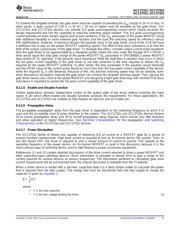
9 Application and Implementation
NOTE
Information in the following applications sections is not part of the TI component
specification, and TI does not warrant its accuracy or completeness. TI’s customers are
responsible for determining suitability of components for their purposes. Customers should
validate and test their design implementation to confirm system functionality.
9.1 Application Information
High-current gate driver devices are required in switching power applications for a variety of reasons. To enable
fast switching of power devices and reduce associated power losses, a powerful gate driver can be employed
between the PWM output of controllers or signal isolation devices and the gates of the power semiconductor
devices. Further, gate drivers are indispensable when sometimes it is just not feasible to have the PWM
controller directly drive the gates of the switching devices. The situation may be encountered because the PWM
signal from a digital controller or signal isolation device is often a 3.3-V or 5-V logic signal which is not capable of
effectively turning on a power switch. A level-shifting circuitry is needed to boost the logic-level signal to the gate-
drive voltage to fully turn on the power device and minimize conduction losses. Traditional buffer drive circuits
based on NPN/PNP bipolar, (or P- N- channel MOSFET), transistors in totem-pole arrangement, being emitter
follower configurations, prove inadequate for this because they lack level-shifting capability and low-drive voltage
protection. Gate drivers effectively combine both the level-shifting and buffer drive functions. Gate drivers may
also minimize the effect of switching noise by locating the high-current driver physically close to the power
switch, drive gate-driver transformers and control floating power device gates, reducing power dissipation and
thermal stress in controllers by absorbing gate-charge power losses.
In summary gate drivers are extremely important components in switching power combining benefits of high-
performance, low-cost, low component count, board-space reduction, and simplified system design.
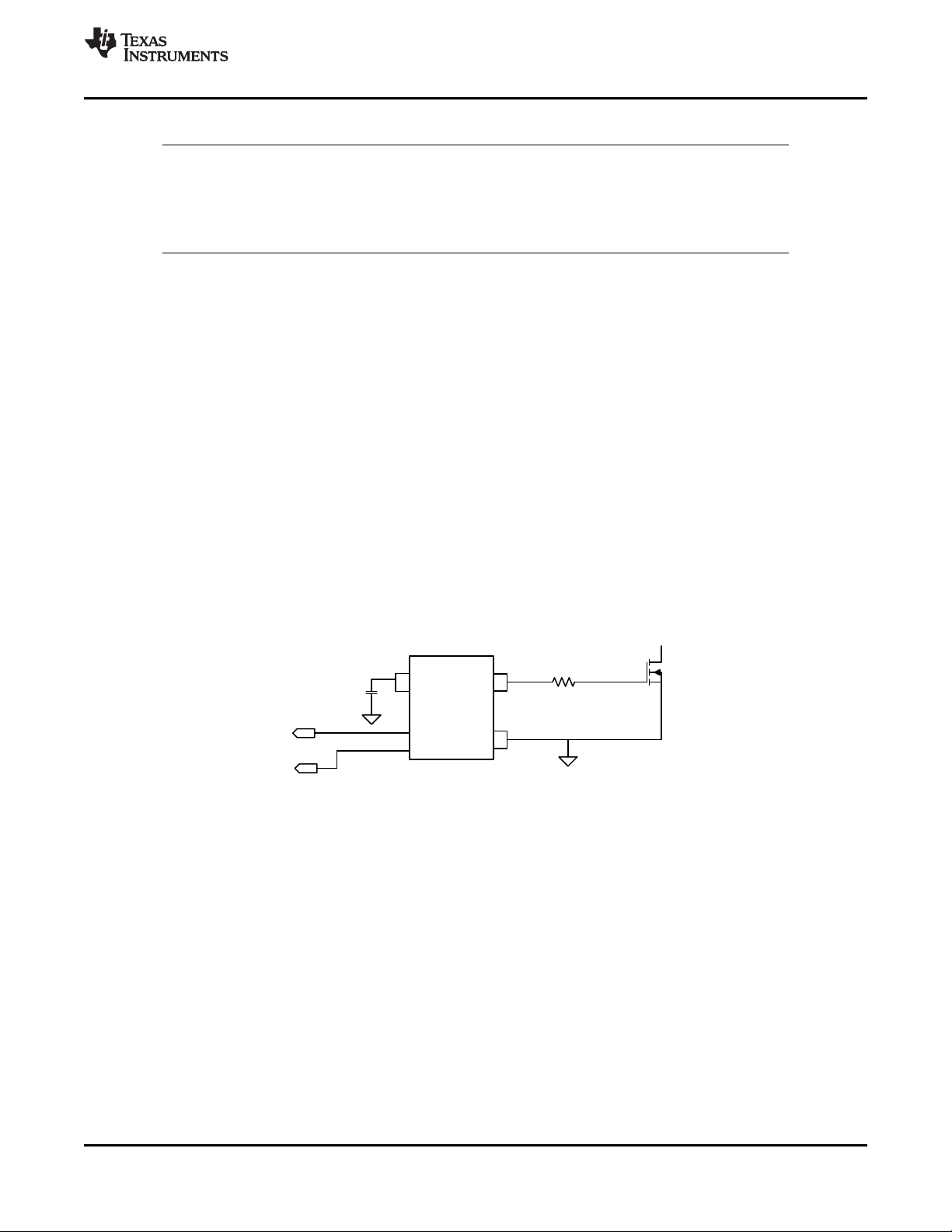
9.2 Typical Application
Figure 27. Typical Application Diagram of UCC27322 and UCC37322
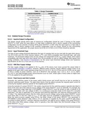
9.2.1 Design Requirements
When selecting the proper gate driver device for an end application, some design considerations must be
evaluated first to make the most appropriate selection. The following design parameters should be used when
selecting the proper gate driver device for an end application: input-to-output configuration, the input threshold
type, bias supply voltage levels, peak source and sink currents, availability of independent enable and disable
functions, propagation delay, power dissipation, and package type. See the example design parameters and
requirements in Table 2.
Copyright © 2002–2016, Texas Instruments Incorporated Submit Documentation Feedback 15
器件 Datasheet 文档搜索
AiEMA 数据库涵盖高达 72,405,303 个元件的数据手册,每天更新 5,000 多个 PDF 文件
