Datasheet 搜索 > FET驱动器 > TI(德州仪器) > UCC27321DGNG4 数据手册 > UCC27321DGNG4 数据手册 16/35 页

¥ 33.78
UCC27321DGNG4 数据手册 - TI(德州仪器)
制造商:
TI(德州仪器)
分类:
FET驱动器
封装:
PowerPad-MSOP-8
描述:
单9A高速低侧MOSFET驱动器与启用 SINGLE 9-A HIGH SPEED LOW-SIDE MOSFET DRIVER WITH ENABLE
Pictures:
3D模型
符号图
焊盘图
引脚图
产品图
页面导航:
引脚图在P3Hot
典型应用电路图在P15
原理图在P1P12
封装尺寸在P23P24P25P27P28
焊盘布局在P20
标记信息在P23P24P25
封装信息在P6P22P23P24P25P26P27P28
技术参数、封装参数在P4
应用领域在P1P26P35
电气规格在P5P16P17
导航目录
UCC27321DGNG4数据手册
Page:
of 35 Go
若手册格式错乱,请下载阅览PDF原文件
UCC27321, UCC27322
UCC37321, UCC37322
SLUS504H –SEPTEMBER 2002–REVISED JANUARY 2016
www.ti.com
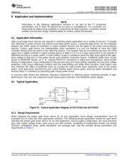
Table 2. Design Parameters
DESIGN PARAMETER EXAMPLE VALUE
Input-to-output configuration Noninverting
Input threshold type CMOS
Bias supply voltage levels 12 V
dVDS/dt
(1)
20 V/ns
Enable function Yes
Propagation delay < 50 ns
Power dissipation < 0.45 W
Package type SOIC (8)
(1) dVDS/dt is a typical requirement for a given design. This value can
be used to find the peak source/sink currents needed as shown in
Peak Source and Sink Currents.
9.2.2 Detailed Design Procedure
9.2.2.1 Input-to-Output Configuration
The design should specify which type of input-to-out configuration should be used. If turning on the power
MOSFET or IGBT when the input signal is in high state is preferred, then a device capable of the noninverting
configuration must be selected. If turning off the power MOSFET or IGBT when the input signal is in high state is
preferred, then a device capable of the inverting configuration must be chosen. Based on this noninverting
requirement of this application, the proper device out of the UCC27322 or UCC37322 should be selected.
9.2.2.2 Input Threshold Type
The type of input voltage threshold determines the type of controller that can be used with the gate driver device.
The UCC2732x and UCC3732x devices feature a TTL and CMOS-compatible input threshold logic, with wide
hysteresis. The threshold voltage levels are low voltage and independent of the V
DD
supply voltage, which allows
compatibility with both logic-level input signals from microcontrollers as well as higher-voltage input signals from
analog controllers. See Electrical Characteristics for the actual input threshold voltage levels and hysteresis
specifications for the UCC2732x and UCC3732x devices.
9.2.2.3 VDD Bias Supply Voltage
The bias supply voltage to be applied to the V
DD
pins of the device must never exceed the values listed in
Recommended Operating Conditions. However, different power switches require different voltage levels to be
applied at the gate. With a wide operating range from 4.5 V to 15 V, the UCC2732x and UCC3732x can be used
to drive a variety of power switches, such as Si MOSFETs (for example, Vgs = 4.5 V, 10 V, 12 V), IGBTs
(V
GE
=15 V), and wide-bandgap power semiconductors (such as GaN, certain types of which allow no higher than
6 V to be applied to the gate terminals).
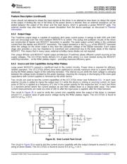
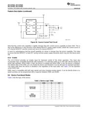
9.2.2.4 Peak Source and Sink Currents
Generally, the switching speed of the power switch during turnon and turnoff must be as fast as possible to
minimize switching power losses. The gate driver device must be able to provide the required peak current for
achieving the targeted switching speeds for the targeted power MOSFET.
Using the example of a power MOSFET, the system requirement for the switching speed is typically described in
terms of the slew rate of the drain-to-source voltage of the power MOSFET (such as dvDS/dt). For example, the
system requirement might state that a SPP20N60C3 power MOSFET must be turned on with a Dvds/dt of 20
V/ns or higher under a DC bus voltage of 400 V in a continuous-conduction-mode (CCM) boost PFC-converter
application. This type of application is an inductive hard-switching application and reducing switching power loss
is critical. This requirement means that the entire drain-to-source voltage swing during power MOSFET turnon
event (from 400 V in the OFF state to V
DS(on)
in ON state) must be completed in approximately 20 ns or less.
When the drain-to-source voltage swing occurs, the Miller charge of the power MOSFET (Q
gd
parameter in
SPP20N60C3 power MOSFET data sheet is 33 nC typically) is supplied by the peak current of gate driver.
According to power MOSFET inductive switching mechanism, the gate-to-source voltage of the power MOSFET
at this time is the Miller plateau voltage, which is typically a few volts higher than the threshold voltage of the
power MOSFET, V
GS(th)
).
16 Submit Documentation Feedback Copyright © 2002–2016, Texas Instruments Incorporated
器件 Datasheet 文档搜索
AiEMA 数据库涵盖高达 72,405,303 个元件的数据手册,每天更新 5,000 多个 PDF 文件
