Datasheet 搜索 > FET驱动器 > TI(德州仪器) > UCC27321DGNG4 数据手册 > UCC27321DGNG4 数据手册 2/35 页

¥ 33.765
UCC27321DGNG4 数据手册 - TI(德州仪器)
制造商:
TI(德州仪器)
分类:
FET驱动器
封装:
PowerPad-MSOP-8
描述:
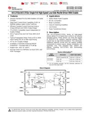
单9A高速低侧MOSFET驱动器与启用 SINGLE 9-A HIGH SPEED LOW-SIDE MOSFET DRIVER WITH ENABLE
Pictures:
3D模型
符号图
焊盘图
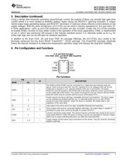
引脚图
产品图
页面导航:
引脚图在P3Hot
典型应用电路图在P15
原理图在P1P12
封装尺寸在P23P24P25P27P28
焊盘布局在P20
标记信息在P23P24P25
封装信息在P6P22P23P24P25P26P27P28
技术参数、封装参数在P4
应用领域在P1P26P35
电气规格在P5P16P17
导航目录
UCC27321DGNG4数据手册
Page:
of 35 Go
若手册格式错乱,请下载阅览PDF原文件

UCC27321, UCC27322
UCC37321, UCC37322
SLUS504H –SEPTEMBER 2002–REVISED JANUARY 2016
www.ti.com
Table of Contents
8.4 Device Functional Modes........................................ 14
1 Features.................................................................. 1
9 Application and Implementation ........................ 15
2 Applications ........................................................... 1
9.1 Application Information............................................ 15
3 Description............................................................. 1
9.2 Typical Application ................................................. 15
4 Revision History..................................................... 2
10 Power Supply Recommendations ..................... 19
5 Description (continued)......................................... 3
11 Layout................................................................... 19
6 Pin Configuration and Functions......................... 3
11.1 Layout Guidelines ................................................. 19
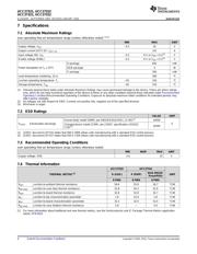
7 Specifications......................................................... 4
11.2 Layout Example .................................................... 20
7.1 Absolute Maximum Ratings...................................... 4
11.3 Thermal Information.............................................. 20
7.2 ESD Ratings.............................................................. 4
12 Device and Documentation Support................. 21
7.3 Recommended Operating Conditions....................... 4
12.1 Device Support...................................................... 21
7.4 Thermal Information.................................................. 4
12.2 Documentation Support ........................................ 21
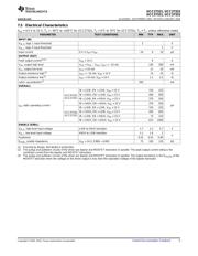
7.5 Electrical Characteristics........................................... 5
12.3 Related Links ........................................................ 21
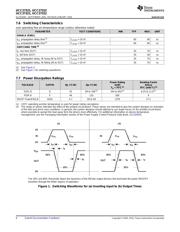
7.6 Switching Characteristics.......................................... 6
12.4 Community Resources.......................................... 21
7.7 Power Dissipation Ratings........................................ 6
12.5 Trademarks........................................................... 21
7.8 Typical Characteristics.............................................. 8
12.6 Electrostatic Discharge Caution............................ 22
8 Detailed Description............................................ 12
12.7 Glossary................................................................ 22
8.1 Overview................................................................. 12
13 Mechanical, Packaging, and Orderable
8.2 Functional Block Diagram....................................... 12
Information........................................................... 22
8.3 Feature Description................................................. 12
4 Revision History
NOTE: Page numbers for previous revisions may differ from page numbers in the current version.
Changes from Revision G (May 2013) to Revision H Page
• Added ESD Ratings table, Feature Description section, Device Functional Modes, Application and Implementation
section, Power Supply Recommendations section, Layout section, Device and Documentation Support section, and
Mechanical, Packaging, and Orderable Information section.................................................................................................. 1
Changes from Revision F (March 2012) to Revision G Page
• Updated AGND pin description. ............................................................................................................................................ 3
• Changed minimum value for input voltage from –5 to –0.3 V in the Absolute Maximum Ratings table. ............................... 4
• Added C
LOAD
= 10 nF to Fall Time vs Supply Voltage graph ................................................................................................. 8
• Changed Changed x-axis values from 1, 10, 100 to 0.1, 1, 10 in Rise Time vs Load Capacitance graph ........................... 8
• Changed Changed x-axis values from 1, 10, 100 to 0.1, 1, 10 in Fall Time vs Output Capacitance graph.......................... 8
2 Submit Documentation Feedback Copyright © 2002–2016, Texas Instruments Incorporated
器件 Datasheet 文档搜索
AiEMA 数据库涵盖高达 72,405,303 个元件的数据手册,每天更新 5,000 多个 PDF 文件
