Datasheet 搜索 > FET驱动器 > TI(德州仪器) > UCC27511DBVR 数据手册 > UCC27511DBVR 数据手册 24/39 页

¥ 2.644
UCC27511DBVR 数据手册 - TI(德州仪器)
制造商:
TI(德州仪器)
分类:
FET驱动器
封装:
SOT-23-6
描述:
TEXAS INSTRUMENTS UCC27511DBVR 驱动器, IGBT, MOSFET, 低压侧, 4.5V-18V电源, 8A输出, -999ms 延迟, SOT-23-6
Pictures:
3D模型
符号图
焊盘图
引脚图
产品图
页面导航:
引脚图在P5P6Hot
典型应用电路图在P1P22P23P24P25P26
原理图在P15P16P17
封装尺寸在P30P32P33
标记信息在P30
封装信息在P7P29P30P31P32P33
功能描述在P4P5
技术参数、封装参数在P7
应用领域在P1P31P39
电气规格在P4P9P19P23
型号编号列表在P4


导航目录
UCC27511DBVR数据手册
Page:
of 39 Go
若手册格式错乱,请下载阅览PDF原文件

UCC27511
,
UCC27512
SLUSAW9F –FEBRUARY 2012–REVISED NOVEMBER 2014
www.ti.com
Typical Application (continued)
10.2.2.4 Peak Source and Sink Currents
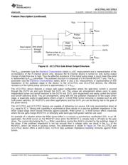
Generally, the switching speed of the power switch during turnon and turnoff should be as fast as possible in
order to minimize switching power losses. The gate driver device must be able to provide the required peak
current for achieving the targeted switching speeds for the targeted power MOSFET.
Using the example of a power MOSFET, the system requirement for the switching speed is typically described in
terms of the slew rate of the drain-to-source voltage of the power MOSFET (such as dV
DS
/dt). For example, the
system requirement might state that a SPP20N60C3 power MOSFET must be turned-on with a dV
DS
/dt of 20
V/ns or higher under a DC bus voltage of 400 V in a continuous-conduction-mode (CCM) boost PFC-converter
application. This type of application is an inductive hard-switching application and reducing switching power
losses is critical. This requirement means that the entire drain-to-source voltage swing during power MOSFET
turn-on event (from 400 V in the OFF state to V
DS(on)
in on state) must be completed in approximately 20 ns or
less. When the drain-to-source voltage swing occurs, the Miller charge of the power MOSFET (Q
GD
parameter in
SPP20N60C3 power MOSFET data sheet = 33 nC typical) is supplied by the peak current of gate driver.
According to power MOSFET inductive switching mechanism, the gate-to-source voltage of the power MOSFET
at this time is the Miller plateau voltage, which is typically a few volts higher than the threshold voltage of the
power MOSFET, V
GS(TH)
.
In order to achieve the targeted dV
DS
/dt, the gate driver must be capable of providing the Q
GD
charge in 20 ns or
less. In other words a peak current of 1.65 A (= 33 nC / 20 ns) or higher must be provided by the gate driver. The
UCC27511 and UCC27512 gate driver is capable of providing 4-A peak sourcing current which clearly exceeds
the design requirement and has the capability to meet the switching speed needed. The 2.4x overdrive capability
provides an extra margin against part-to-part variations in the Q
GD
parameter of the power MOSFET along with
additional flexibility to insert external gate resistors and fine tune the switching speed for efficiency versus EMI
optimizations.
However, in practical designs the parasitic trace inductance in the gate drive circuit of the PCB will have a
definitive role to play on the power MOSFET switching speed. The effect of this trace inductance is to limit the
dI/dt of the output current pulse of the gate driver. In order to illustrate this, consider output current pulse
waveform from the gate driver to be approximated to a triangular profile, where the area under the triangle (½ ×
I
PEAK
× time) would equal the total gate charge of the power MOSFET (Q
G
parameter in SPP20N60C3 power
MOSFET datasheet = 87 nC typical). If the parasitic trace inductance limits the dI/dt then a situation may occur in
which the full peak current capability of the gate driver is not fully achieved in the time required to deliver the QG
required for the power MOSFET switching. In other words the time parameter in the equation would dominate
and the I
PEAK
value of the current pulse would be much less than the true peak current capability of the device,
while the required QG is still delivered. Because of this, the desired switching speed may not be realized, even
when theoretical calculations indicate the gate driver is capable of achieving the targeted switching speed. Thus,
placing the gate driver device very close to the power MOSFET and designing a tight gate drive-loop with
minimal PCB trace inductance is important to realize the full peak-current capability of the gate driver.
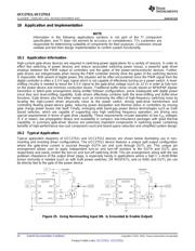
10.2.2.5 Enable and Disable Function
Certain applications demand independent control of the output state of the driver without involving the input
signal. A pin which offers an enable and disable function achieves this requirement. The UCC27511 and
UCC27512 devices offer 2 input pins, IN+ and IN–, both of which control the state of the output as listed in
Table 3. Based on whether an inverting or noninverting input signal is provided to the driver, the appropriate
input pin can be selected as the primary input for controlling the gate driver. The other unused input pin can be
conveniently used for the enable and disable functionality. If the design does not require an enable function, the
unused input pin can be tied to either the V
DD
pin (in case IN+ is the unused pin), or GND (in case IN– is unused
pin) in order to ensure it does not affect the output status.
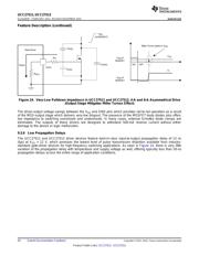
10.2.2.6 Propagation Delay
The acceptable propagation delay from the gate driver is dependent on the switching frequency at which it is
used and the acceptable level of pulse distortion to the system. The UCC27511 and UCC27512 devices feature
industry best-in-class 13-ns (typical) propagation delays which ensures very little pulse distortion and allows
operation at very high-frequencies. See the table for the propagation and switching characteristics of the
UCC27511 and UCC27512 devices.
24 Submit Documentation Feedback Copyright © 2012–2014, Texas Instruments Incorporated
Product Folder Links: UCC27511 UCC27512
器件 Datasheet 文档搜索
AiEMA 数据库涵盖高达 72,405,303 个元件的数据手册,每天更新 5,000 多个 PDF 文件
