Datasheet 搜索 > FET驱动器 > TI(德州仪器) > UCC27511DBVT 数据手册 > UCC27511DBVT 数据手册 25/39 页

¥ 4.344
UCC27511DBVT 数据手册 - TI(德州仪器)
制造商:
TI(德州仪器)
分类:
FET驱动器
封装:
SOT-23-6
描述:
TEXAS INSTRUMENTS UCC27511DBVT 芯片, MOSFET驱动器, 低压侧, 6-SOT-23
Pictures:
3D模型
符号图
焊盘图
引脚图
产品图
页面导航:
引脚图在P5P6Hot
典型应用电路图在P1P22P23P24P25P26
原理图在P15P16P17
封装尺寸在P30P32P33
标记信息在P30
封装信息在P7P29P30P31P32P33
功能描述在P4P5
技术参数、封装参数在P7
应用领域在P1P31P39
电气规格在P4P9P19P23
型号编号列表在P4
导航目录
UCC27511DBVT数据手册
Page:
of 39 Go
若手册格式错乱,请下载阅览PDF原文件

2
G LOAD DD SW g DD SW
P C V f Q V f= =
2
G LOAD DD SW
P C V f=
2
G LOAD DD
1
E C V
2
=
DISS DC SW
P P P= +
UCC27511
,
UCC27512
www.ti.com
SLUSAW9F –FEBRUARY 2012–REVISED NOVEMBER 2014
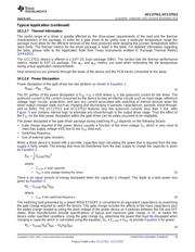
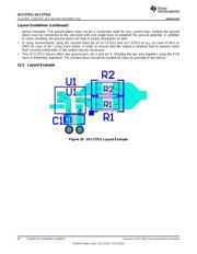
Typical Application (continued)
10.2.2.7 Thermal Information
The useful range of a driver is greatly affected by the drive-power requirements of the load and the thermal
characteristics of the package. In order for a gate driver to be useful over a particular temperature range the
package must allow for the efficient removal of the heat produced while keeping the junction temperature within
rated limits. The thermal metrics for the driver package is listed in the table. For detailed information regarding
the table, please refer to the Application Note from Texas Instruments entitled IC Package Thermal Metrics
(SPRA953).
The UCC27511 device is offered in a SOT-23, 6-pin package (DBV). The section lists the thermal performance
metrics related to SOT-23 package. The ψ
JT
and ψ
JB
metrics are used when estimating the die temperature
during actual application measurements.
Heat removal occurs primarily through the leads of the device and the PCB traces connected to the leads.
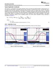
10.2.2.8 Power Dissipation
Power dissipation of the gate driver has two portions as shown in Equation 1.
(1)
The DC portion of the power dissipation is P
DC
= I
Q
x VDD where I
Q
is the quiescent current for the driver. The
quiescent current is the current consumed by the device to bias all internal circuits such as input stage, reference
voltage, logic circuits, protections, and also any current associated with switching of internal devices when the
driver output changes state (such as charging and discharging of parasitic capacitances, parasitic shoot-through,
and so forth). The UCC27511 and UCC27512 features very low quiescent currents (less than 1 mA, refer
Figure 7) and contains internal logic to eliminate any shoot-through in the output driver stage. Thus the effect of
the P
DC
on the total power dissipation within the gate driver can be safely assumed to be negligible.
The power dissipated in the gate-driver package during switching (P
SW
) depends on the following factors:
• Gate charge required of the power device (usually a function of the drive voltage V
G
, which is very close to
input bias supply voltage VDD due to low V
OH
drop-out).
• Switching frequency.
• Use of external gate resistors.
When a driver device is tested with a discrete, capacitive load calculating the power that is required from the bias
supply is fairly simple. The energy that must be transferred from the bias supply to charge the capacitor is given
by Equation 2.
where
• C
LOAD
is load capacitor
• V
DD
is bias voltage feeding the driver (2)
There is an equal amount of energy dissipated when the capacitor is charged. This leads to a total power loss
given by Equation 3.
where
• ƒ
SW
is the switching frequency (3)
The switching load presented by a power MOSFET/IGBT is converted to an equivalent capacitance by examining
the gate charge required to switch the device. This gate charge includes the effects of the input capacitance plus
the added charge needed to swing the drain voltage of the power device as it switches between the ON and OFF
states. Most manufacturers provide specifications of typical and maximum gate charge, in nC, to switch the
device under specified conditions. Using the gate charge Qg, determine the power that must be dissipated when
charging a capacitor which is calculated using the equation, Q
G
= C
LOAD
x V
DD
, to provide Equation 4 for power.
(4)
Copyright © 2012–2014, Texas Instruments Incorporated Submit Documentation Feedback 25
Product Folder Links: UCC27511 UCC27512
器件 Datasheet 文档搜索
AiEMA 数据库涵盖高达 72,405,303 个元件的数据手册,每天更新 5,000 多个 PDF 文件
