Datasheet 搜索 > PWM控制器 > TI(德州仪器) > UCC2806DW 数据手册 > UCC2806DW 数据手册 5/32 页
 器件3D模型
¥ 81.581
UCC2806DW 数据手册 - TI(德州仪器)
制造商:
TI(德州仪器)
分类:
PWM控制器
封装:
SOIC-16
描述:
UCC28/UCC38 系列,Texas Instruments隔离式回扫电源控制器提供恒定电压 (CV) 和恒定电流 (CC) 输出调节,用于提高对较大负载阶跃的瞬时响应。 初级侧调节 (PSR) 无需光耦合器。### 回扫控制器,Texas Instruments电流模式和电压模式 PWM 控制器 初级侧调节 峰值功率模式 低功率
Pictures:
3D模型
符号图
焊盘图
引脚图
产品图
页面导航:
引脚图在P6P7Hot
典型应用电路图在P9
原理图在P8
封装尺寸在P12P13P15P16P17P19P20
型号编码规则在P3
标记信息在P15P16P17
封装信息在P12P13P14P15P16P17P18P19P20
技术参数、封装参数在P2
应用领域在P18P32
电气规格在P3P4P5
导航目录
UCC2806DW数据手册
Page:
of 32 Go
若手册格式错乱,请下载阅览PDF原文件
UCC1806
UCC2806
UCC3806
SLUS272F -- FEBRUARY 2000 -- REVISED AUGUST 2006
5
www.ti.com
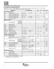
ELECTRICAL CHARACTERISTICS
V
IN
=12V,R
T
=33kΩ,C
T
= 330 pF, C
BYPASS
on V
REF
=0.01μF, -- 5 5°C to 125°C for the UCC1806, --40°C<T
A
<85°C for the UCC2806,
0°C<T
A
<70°C for the UCC3806, and T
A
=T
J
(unless otherwise noted)
SHUTDOWN TERMINAL
Threshold volta
g
e
UCC1806
UCC2806
0.94 1.00 1.06
V
T
h
r
e
s
h
o
l
d
v
o
l
t
a
g
e
UCC3806 0.9 1.0 1.1
V
Input voltage range 0 V
IN
t
DLY
Delay-to-output time 0V≤ V
SHUTDOWN
≤ 1.3 V 75 150 ns
OUTPUT
Output supply voltage 2.5 15.0
UCC1806
I
SINK
=20mA 100 300
L
o
w
l
e
v
e
l
o
u
t
p
u
t
v
o
l
t
a
g
e
U
C
C
1
8
0
6
UCC2806
I
SINK
= 100 mA 0.4 1.1
Low-level output voltage
U
C
C
3
8
0
6
I
SINK
=20mA 100 200
V
UCC3806
I
SINK
= 100 mA 0.4 1.1
V
H
i
g
h
l
e
v
e
l
o
u
t
p
u
t
v
o
l
t
a
g
e
I
SRC
=--20mA 11.6 11.9
High-level output voltage
I
SRC
= --100 mA 11.0 11.6
t
RISE
Rise time T
J
=25°C, C
LOAD
= 1000 pF 35 65
n
s
t
FALL
Fall time T
J
=25°C, C
LOAD
= 1000 pF 35 65
ns
UNDERVOLTAGE LOCKOUT (UVLO)
V
START
Startup threshold voltage 6.5 7.5 8.0 V
Threshold hysteresis 0.75 V
I
START
Startup current V
IN
<V
START
50 100 μA
I Operating supply current 1.0 1.4 mA
V
IN
shunt voltage I
VIN
=10mA 15.0 17.5
(1)
Line range = 10 V to 15 V, load range = 0.2 mA to 5 mA
(2)
Ensured by design. Not production tested.
(3)
Parameters measured at trip point of latch with V
NI
=VREF,V
INV
=0V.
(4)
Amplifier gain defined as: G = delta change at COMP /delta change forced at CS+ delta voltage at CS+ = 0 to 1V
(5)
Current-sense amplifier output is slew rate limited to provide noise immunity.
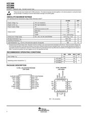
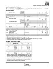
THERMAL RESISTANCE TABLE
PACKAGE
DESIGNATOR
PACKAGE TYPE
θ
JC
(°C/W)
θ
JA
(°C/W)
D SOIC --16 35 50 to 120
(1)
DW SOICW--16 27 50 to 100
(1)
J CDIP--16 28 80 to 120
L CLCC--20 20 70 to 80
M SSOP--16 38 144 to 172
(2)
N PDIP--16 45 90
(1)
PW TSSOP --16 15 123 to 147
(2)
Q PLCC--20 34 43 to 75
(1)
(1)
Specified θ
JA
(junction to ambient) is for devices mounted to 5 in
2
FR4 PC board
with one ounce copper where noted. When resistance range is given, lower values
are for 5 in
2
aluminum PC board. Test PWB was 0.062 in thick and typically used
0.635 mm trace widths for power packages and 1.3 mm trace widths for non-power
packages with a 100x100 mil probe land area at the end of each trace.
(2)
Modeled data. If value range given for θ
JA
, the lower value is for 3x3 inch1 oz
internal copper ground plane, and the higher value is for 1x1 inch ground plane. All
model data assumes only one trace for each non-fused lead.
器件 Datasheet 文档搜索
AiEMA 数据库涵盖高达 72,405,303 个元件的数据手册,每天更新 5,000 多个 PDF 文件
