Datasheet 搜索 > PWM控制器 > TI(德州仪器) > UCC2806DW 数据手册 > UCC2806DW 数据手册 6/32 页
 器件3D模型
¥ 81.581
UCC2806DW 数据手册 - TI(德州仪器)
制造商:
TI(德州仪器)
分类:
PWM控制器
封装:
SOIC-16
描述:
UCC28/UCC38 系列,Texas Instruments隔离式回扫电源控制器提供恒定电压 (CV) 和恒定电流 (CC) 输出调节,用于提高对较大负载阶跃的瞬时响应。 初级侧调节 (PSR) 无需光耦合器。### 回扫控制器,Texas Instruments电流模式和电压模式 PWM 控制器 初级侧调节 峰值功率模式 低功率
Pictures:
3D模型
符号图
焊盘图
引脚图
产品图
页面导航:
引脚图在P6P7Hot
典型应用电路图在P9
原理图在P8
封装尺寸在P12P13P15P16P17P19P20
型号编码规则在P3
标记信息在P15P16P17
封装信息在P12P13P14P15P16P17P18P19P20
技术参数、封装参数在P2
应用领域在P18P32
电气规格在P3P4P5
导航目录
UCC2806DW数据手册
Page:
of 32 Go
若手册格式错乱,请下载阅览PDF原文件

UCC1806
UCC2806
UCC3806
SLUS272F -- FEBRUARY 2000 -- REVISED AUGUST 2006
6
www.ti.com
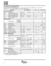
TERMINAL FUNCTIONS
TERMINAL
PACKAGES
I
/
O
D
E
S
C
R
I
P
T
I
O
N
NAME
D/DW/J/M
/N/PW
L,Q
I
/
O
D
E
S
C
R
I
P
T
I
O
N
AOUT 11 14
O
H
i
g
h
c
u
r
r
e
n
t
g
a
t
e
d
r
i
v
e
f
o
r
t
h
e
e
x
t
e
r
n
a
l
M
O
S
F
E
T
s
BOUT 14 18
O High-current gate drive
f
or the e
x
ternal MOSFETs
COMP 7 9 O Output of the error amplifier
CS-- 3 4 I Inverting input of the 3×, differential current sense amplifier
CS+ 4 5 I Non-inverting input of the 3×, differential current sense amplifier
CT 8 10 I Oscillator timing capacitor connection point
CURLIM 1 2 I
Programs the primary current limit threshold that determins latching or retry after an
overcurrent situation
GND 12 15 -- Reference ground and power ground for all functions of this device
INV 6 8 I Inverting input of the error amplifier.
NI 5 7 I Non-nverting input of the error amplifier.
RT 9 12 I Connection point for the oscillator timing resistor
SHUTDOWN 16 20 I
Provided for enhanced protection. When SHUTDOWN is driven above 1 V, AOUT and
BOUT are forced low.
SYNC 10 13 I/O Allows providing external synchronization with TTL compatible thresholds.
VC 13 17 I Input supply connection for the FET drive outputs.
VIN 15 19 I Input supply connection for this device.
VREF 2 3 O Reference output.
DETAILED PIN DESCRIPTIONS
AOUT and BOUT: AOUT and BOUT provide alternating high current gate drive for the external MOSFETs. Duty
cycle can be varied from 0% to 50% where minimum dead time is a function of CT. Both outputs use MOS
transistor switches with inherent anti-parallel body diodes to clamp voltage swings to the supply rails, allowing
operation without the use of clamp diodes.
COMP: COMP is the output of the error amplifier and the input of the PWM comparator. The error amplifier is
a low output impedance, 2-MHz operational amplifier which allows sinking or sourcing of current at the COMP
pin. The error amplifier is internally current limited, so that zero duty cycle can be commanded by externally
forcingCOMPtoGND.
CS--: C S-- is the inverting input of the 3× differential current sense amplifier.
CS+: CS+ is the non-inverting input of the 3× differential current sense amplifier.
CT: CT is the oscillator timing capacitor connection point, which is charged by the current set by RT. CT is
discharged to GND through a 2.5-mA current sink. This causes a linear discharge of CT to 0 V which then
initiates the next switching cycle. Dead time occurs during the discharge of CT, forcing AOUT and BOUT low.
Switching frequency (f
S
) and dead time (t
D
) are approximated by:
f
S
=
1
1.96 × R
T
× C
T
+ t
D
and t
D
= 956 × C
T
(1)
器件 Datasheet 文档搜索
AiEMA 数据库涵盖高达 72,405,303 个元件的数据手册,每天更新 5,000 多个 PDF 文件
