Datasheet 搜索 > 稳压芯片 > TI(德州仪器) > UCC2813QPWR-3Q1 数据手册 > UCC2813QPWR-3Q1 数据手册 3/20 页
 器件3D模型
¥ 8.92
UCC2813QPWR-3Q1 数据手册 - TI(德州仪器)
制造商:
TI(德州仪器)
分类:
稳压芯片
封装:
TSSOP-8
描述:
具有 4.1V/3.6V UVLO 和 100% 占空比的汽车类经济型单端 1MHz 电流模式 PWM 控制器 8-TSSOP -40 to 125
Pictures:
3D模型
符号图
焊盘图
引脚图
产品图
页面导航:
导航目录
UCC2813QPWR-3Q1数据手册
Page:
of 20 Go
若手册格式错乱,请下载阅览PDF原文件
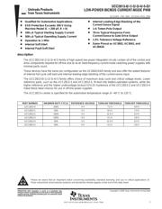
SGLS245D − MAY 2004 − REVISED APRIL 2008
3
POST OFFICE BOX 655303 • DALLAS, TEXAS 75265
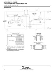
ordering information
UCC2813-
QD
Package
D = Plastic SOIC, PW = Plastic TSSOP
Product Option
0 through 5
Automotive Temperature Range Indicator
R
Tape and Reel Indicator
0
absolute maximum ratings over operating free-air temperature range (unless otherwise noted)
†‡
V
CC
voltage
w
12 V. . . . . . . . . . . . . . . . . . . . . . . . . . . . . . . . . . . . . . . . . . . . . . . . . . . . . . . . . . . . . . . . . . . . . . . . . . . . .
V
CC
current
w
30 mA. . . . . . . . . . . . . . . . . . . . . . . . . . . . . . . . . . . . . . . . . . . . . . . . . . . . . . . . . . . . . . . . . . . . . . . . . . .
Output current, I
O
±1 A. . . . . . . . . . . . . . . . . . . . . . . . . . . . . . . . . . . . . . . . . . . . . . . . . . . . . . . . . . . . . . . . . . . . . . . . .
Output energy (capacitive load) 20 µJ. . . . . . . . . . . . . . . . . . . . . . . . . . . . . . . . . . . . . . . . . . . . . . . . . . . . . . . . . . . . .
Analog inputs (FB, CS) −0.3 V to 6.3 V. . . . . . . . . . . . . . . . . . . . . . . . . . . . . . . . . . . . . . . . . . . . . . . . . . . . . . . . . . . .
Power dissipation at T
A
< +25_C (D package) 0.65 W. . . . . . . . . . . . . . . . . . . . . . . . . . . . . . . . . . . . . . . . . . . . . .
Storage temperature range, T
stg
−65_C to 150_C. . . . . . . . . . . . . . . . . . . . . . . . . . . . . . . . . . . . . . . . . . . . . . . . . . . .
Lead temperature soldering 1,6 mm (1/16 inch) from case for 10 seconds 300_C. . . . . . . . . . . . . . . . . . . . . . .
†
Stresses beyond those listed under “absolute maximum ratings” may cause permanent damage to the device. These are stress ratings only, and
functional operation of the device at these or any other conditions beyond those indicated under “recommended operating conditions” is not
implied. Exposure to absolute-maximum-rated conditions for extended periods may affect device reliability.
‡
Unless otherwise indicated, voltages are reference to ground and currents are positive into and negative out of the specified terminals.
w In normal operation V
CC
is powered through a current limiting resistor. Absolute maximum of 12 V applies when V
CC
is driven from a low
impedance source such that I
CC
does not exceed 30 mA (which includes gate drive current requirement).
electrical characteristics T
A
= −40_C to 125_C, V
CC
= 10 V (see Note 1), RT = 100 kΩ from REF to
RC, CT = 330 pF from RC to GND, 0.1-F capacitor from V
CC
to GND, 0.1-F capacitor from V
REF
to
GND, and T
A
= T
J
(unless otherwise noted)
PARAMETER TEST CONDITIONS MIN TYP MAX UNIT
Reference Section
Output voltage
T
J
= 25_C, I = 0.2 mA
UCC2813-0/-1/-2/-4 4.925 5 5.075
V
Output voltage
T
J
= 25_C, I = 0.2 mA
UCC2813-3/-5 3.94 4 4.06
V
Load regulation voltage I = 0.2 mA to 5 mA 10 30 mV
Total variation voltage
See Note 5
UCC2813-0/-1/-2/-4 4.84 5 5.1
V
Total variation voltage See Note 5
UCC2813-3/-5 3.84 4 4.08
V
Output noise voltage
f = 10 Hz to 10 kHz,
See Note 7
T
J
= 25_C 70 µV
Long term stability
1000 hours,
See Note 7
T
A
= 125_C 5 mV
Output short-circuit current −5 −35 mA
器件 Datasheet 文档搜索
AiEMA 数据库涵盖高达 72,405,303 个元件的数据手册,每天更新 5,000 多个 PDF 文件
