Datasheet 搜索 > 稳压芯片 > TI(德州仪器) > UCC2813QPWR-3Q1 数据手册 > UCC2813QPWR-3Q1 数据手册 6/20 页
 器件3D模型
¥ 8.92
UCC2813QPWR-3Q1 数据手册 - TI(德州仪器)
制造商:
TI(德州仪器)
分类:
稳压芯片
封装:
TSSOP-8
描述:
具有 4.1V/3.6V UVLO 和 100% 占空比的汽车类经济型单端 1MHz 电流模式 PWM 控制器 8-TSSOP -40 to 125
Pictures:
3D模型
符号图
焊盘图
引脚图
产品图
页面导航:

导航目录
UCC2813QPWR-3Q1数据手册
Page:
of 20 Go
若手册格式错乱,请下载阅览PDF原文件
SGLS245D − MAY 2004 − REVISED APRIL 2008
6
POST OFFICE BOX 655303 • DALLAS, TEXAS 75265
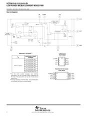
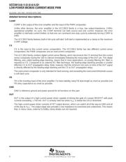
detailed terminal descriptions
COMP
COMP is the output of the error amplifier and the input of the PWM comparator.
Unlike other devices, the error amplifier in the UCC2813 family is a true, low output-impedance, 2-MHz
operational amplifier. As such, the COMP terminal can both source and sink current. However, the error
amplifier is internally current limited, so that one can command zero duty cycle by externally forcing COMP to
GND.
The UCC2813 family features built-in full-cycle soft start. Soft start is implemented as a clamp on the maximum
COMP voltage.
CS
CS is the input to the current sense comparators. The UCC2813 family has two different current sense
comparators: the PWM comparator and an overcurrent comparator.
The UCC2813 family contains digital current sense filtering, which disconnects the CS terminal from the current
sense comparator during the 100 ns interval immediately following the rising edge of the OUT pin. This digital
filtering, also called leading-edge blanking, means that in most applications, no analog filtering (RC filter) is
required on CS. Compared to an external RC filter technique, the leading-edge blanking provides a smaller
effective CS to OUT propagation delay. Note, however, that the minimum non-zero on time of the OUT signal
is directly affected by the leading-edge blanking and the CS to OUT propagation delay.
The overcurrent comparator is only intended for fault sensing, and exceeding the overcurrent threshold causes
a soft start cycle.
FB
FB is the inverting input of the error amplifier. For best stability, keep FB lead length as short as possible and
FB stray capacitance as small as possible.
GND
GND is reference ground and power ground for all functions on this part.
OUT
OUT is the output of a high-current power driver capable of driving the gate of a power MOSFET with peak
currents exceeding "750 mA. OUT is actively held low when V
CC
is below the UVLO threshold.
The high-current power driver consists of FET output devices, which can switch all of the way to GND and all
of the way to V
CC
. The output stage also provides a low impedance to overshoot and undershoot. This means
that, in many cases, external Schottky clamp diodes are not required.
器件 Datasheet 文档搜索
AiEMA 数据库涵盖高达 72,405,303 个元件的数据手册,每天更新 5,000 多个 PDF 文件
