Datasheet 搜索 > 稳压芯片 > TI(德州仪器) > UCC38085PWR 数据手册 > UCC38085PWR 数据手册 10/19 页
 器件3D模型
¥ 0
UCC38085PWR 数据手册 - TI(德州仪器)
制造商:
TI(德州仪器)
分类:
稳压芯片
封装:
TSSOP-8
Pictures:
3D模型
符号图
焊盘图
引脚图
产品图
页面导航:
原理图在P7P11
型号编码规则在P2
应用领域在P1P19
导航目录
UCC38085PWR数据手册
Page:
of 19 Go
若手册格式错乱,请下载阅览PDF原文件
SLUS488B − SEPTEMBER 2002 − REVISED MAY 2003
10
www.ti.com
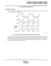
layout considerations
To prevent noise problems, bypass VDD to GND with a ceramic capacitor as close to the chip as possible along
with an electrolytic capacitor. A 1-µF decoupling capacitor is recommended.
Use a local ground plane near the small signal pins (CTRL, ISET, CS and RT) of the IC for shielding. Connect
the local ground plane to the GND pin with a single trace. Do not extend the local ground plane under the power
pins (VDD, OUTA, OUTB and GND). Instead, use signal return traces to the GND pin for ground returns on the
side of the integrated circuit with the power pins.
For best performance, keep the timing resistor lead from RT pin (pin 4) to GND (pin 5) as short as possible.
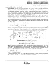
special layout considerations for the TSSOP package
Due to the different pinout and smaller lead pitch of the TSSOP package, special attention must be paid to
minimize noise problems. The pinout is different because the device had to be rotated 90° to fit into the smaller
TSSOP package.
For example, the two output pins are now on opposite sides of the package. The traces should not run under
the package together as they will couple switching noise into analog pins.
Another common problem is when RT and OUTB (pins 6 and 8) are routed together for some distance even
though they are not immediate side by side pins. Because of this, when OUTB rises, a voltage spike of upto
400 mV can couple into the RT. This spike causes the internal charge current into CT to be turned off
momentarily resulting in lower duty cycle. It is also important that note that the RT pin voltage cannot be
stabilized with a capacitor. The RT pin is just a dc voltage to program the internal CT. Instead, keep the OUTB
and RT runs short and far from each other and follow the printed wiring board layout suggestions above to fix
the problem.
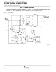
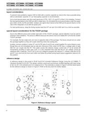
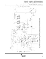
reference design
A reference design is discussed in 50-W Push-Pull Converter Reference Design Using the UCC38083, TI
Literature Number SLUU135. This design controls a push-pull synchronous rectified topology with input range
of 18 V to 35 V (24 nominal) and 3.3-V output at 15 A. The schematic is shown in Figure 5 and the board layout
for the reference design is shown in Figure 4. Refer to the document for further details.
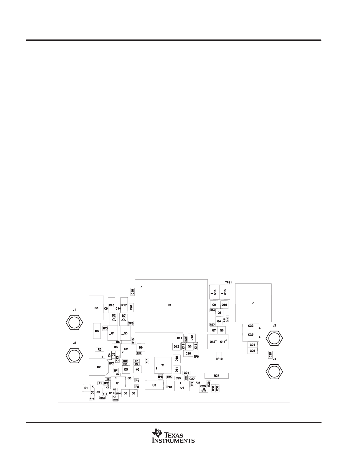
Figure 4. Reference Design Layout
器件 Datasheet 文档搜索
AiEMA 数据库涵盖高达 72,405,303 个元件的数据手册,每天更新 5,000 多个 PDF 文件
