Datasheet 搜索 > 稳压芯片 > TI(德州仪器) > UCC38085PWR 数据手册 > UCC38085PWR 数据手册 7/19 页
 器件3D模型
¥ 0
UCC38085PWR 数据手册 - TI(德州仪器)
制造商:
TI(德州仪器)
分类:
稳压芯片
封装:
TSSOP-8
Pictures:
3D模型
符号图
焊盘图
引脚图
产品图
页面导航:
原理图在P7P11
型号编码规则在P2
应用领域在P1P19
导航目录
UCC38085PWR数据手册
Page:
of 19 Go
若手册格式错乱,请下载阅览PDF原文件
SLUS488B − SEPTEMBER 2002 − REVISED MAY 2003
7
www.ti.com
detailed pin descriptions (continued)
OUTA and OUTB: Alternating high-current output stages. Both stages are capable of driving the gate of a power
MOSFET. Each stage is capable of 500-mA peak-source current, and 1-A peak-sink current.
The output stages switch at half the oscillator frequency, in a push-pull configuration. When the voltage on the
internal oscillator capacitor is rising, one of the two outputs is high, but during fall time, both outputs are off. This
dead time between the two outputs, along with a slower output rise time than fall time, ensures that the two
outputs cannot be on at the same time. This dead time is typically 110 ns.
The high-current output drivers consist of MOSFET output devices, which switch from VDD to GND. Each output
stage also provides a very low impedance to overshoot and undershoot. This means that in many cases,
external Schottky clamp diodes are not required.
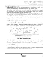
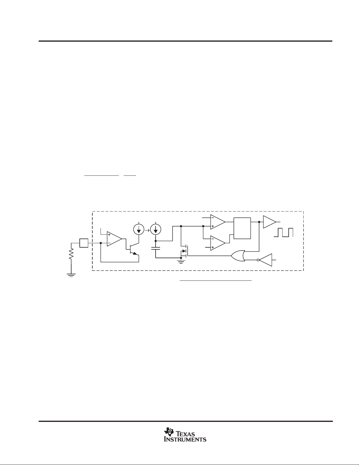
RT: The oscillator programming pin. The oscillator features an internal timing capacitor. An external resistor,
R
T
, sets a current from the RT pin to ground. Due to variations in the internal C
T
, nominal V
RT
of 1.5 V can vary
from 1.2 V to 1.6 V
Selecting RT as shown programs the oscillator frequency:
RT +
1
28.7 10
−12
ǒ
1
f
OSC
* 2.0 10
−7
Ǔ
where f
OSC
is in Hz, resistance in Ω. The recommended range of timing resistors is between 25 kΩ and 698 kΩ.
For best performance, keep the timing resistor lead from the RT pin to GND (pin 5) as short as possible.
UDG−01083
Approximate Frequency +
1
28.7 10
−12
R
T
)
ǒ
2.0 10
−7
Ǔ
4
1.5 V
0.2 V
SQ
R
I
RT
I
CT
C
T
1.5 V
OSCILLATOR
OUTPUT
R
T
Figure 2. Block Diagram for Oscillator
VDD: The power input connection for this device. Although quiescent VDD current is very low, total supply
current may be higher, depending on OUTA and OUTB current, and the programmed oscillator frequency. Total
VDD current is the sum of quiescent VDD current and the average OUT current. Knowing the operating
frequency and the MOSFET gate charge (Q
G
), average OUT current can be calculated from:
I
OUT
+ Q
G
f
OSC
where f is the oscillator frequency.
To prevent noise problems, bypass VDD to GND with a ceramic capacitor as close to the chip as possible along
with an electrolytic capacitor. A 1-µF decoupling capacitor is recommended.
(3)
(4)
器件 Datasheet 文档搜索
AiEMA 数据库涵盖高达 72,405,303 个元件的数据手册,每天更新 5,000 多个 PDF 文件
