Datasheet 搜索 > EEPROM芯片 > Xilinx(赛灵思) > XCF02SVOG20C 数据手册 > XCF02SVOG20C 数据手册 26/35 页
 器件3D模型
¥ 74.198
XCF02SVOG20C 数据手册 - Xilinx(赛灵思)
制造商:
Xilinx(赛灵思)
分类:
EEPROM芯片
封装:
TSSOP-20
描述:
XILINX XCF02SVOG20C 芯片, 存储器, PROM, 闪存平台, 2Mb, 20TSSOP
Pictures:
3D模型
符号图
焊盘图
引脚图
产品图
页面导航:
引脚图在P24P25P26P27P28Hot
原理图在P2P34
型号编码规则在P30
标记信息在P30P31P34
封装信息在P13
技术参数、封装参数在P13P24P33
电气规格在P1P13P16P33
导航目录
XCF02SVOG20C数据手册
Page:
of 35 Go
若手册格式错乱,请下载阅览PDF原文件
Platform Flash In-System Programmable Configuration PROMs
DS123 (v2.19) June 6, 2016 www.xilinx.com
Product Specification 26
R
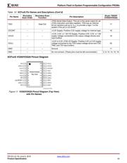
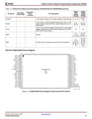
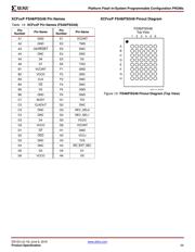
XCFxxP Pinouts and Pin Descriptions
XCFxxP VO48/VOG48 and FS48/FSG48 Pin Names and Descriptions
Table 13 provides a list of the pin names and descriptions for the XCFxxP 48-pin VO48/VOG48 and 48-pin
FS48/FSG48 packages.
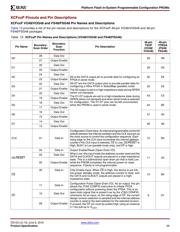
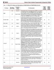
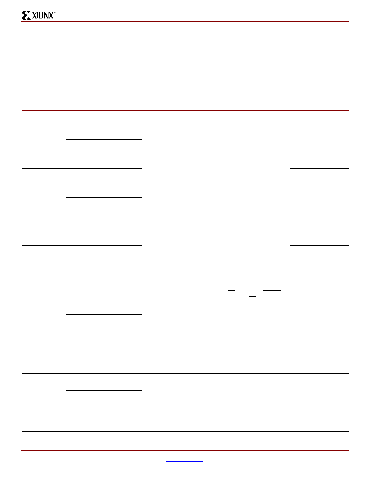
Table 13: XCFxxP Pin Names and Descriptions (VO48/VOG48 and FS48/FSG48)
Pin Name
Boundary-
Scan Order
Boundary-
Scan
Function
Pin Description
48-pin
TSOP
(VO48/
VOG48)
48-pin
TFBGA
(FS48/
FSG48)
D0
28 Data Out
D0 is the DATA output pin to provide data for configuring an
FPGA in serial mode.
D0-D7 are the DATA output pins to provide parallel data for
configuring a Xilinx FPGA in SelectMap (parallel) mode.
The D0 output is set to a high-impedance state during ISPEN
(when not clamped).
The D1-D7 outputs are set to a high-impedance state during
ISPEN (when not clamped) and when serial mode is selected
for configuration. The D1-D7 pins can be left unconnected
when the PROM is used in serial mode.
28 H6
27 Output Enable
D1
26 Data Out
29 H5
25 Output Enable
D2
24 Data Out
32 E5
23 Output Enable
D3
22 Data Out
33 D5
21 Output Enable
D4
20 Data Out
43 C5
19 Output Enable
D5
18 Data Out
44 B5
17 Output Enable
D6
16 Data Out
47 A5
15 Output Enable
D7
14 Data Out
48 A6
13 Output Enable
CLK 01 Data In
Configuration Clock Input. An internal programmable control bit
selects between the internal oscillator and the CLK input pin as
the clock source to control the configuration sequence. Each
rising edge on the CLK input increments the internal address
counter if the CLK input is selected, CE
is Low, OE/RESET is
High, BUSY is Low (parallel mode only), and CF
is High.
12 B3
OE/RESET
04 Data In Output Enable/Reset (Open-Drain I/O).
When Low, this input holds the address counter reset and the
DATA and CLKOUT outputs are placed in a high-impedance
state. This is a bidirectional open-drain pin that is held Low
while the PROM completes the internal power-on reset
sequence. Polarity is not programmable.
11 A3
03 Data Out
02 Output Enable
CE
00 Data In Chip Enable Input. When CE is High, the device is put into
low-power standby mode, the address counter is reset, and
the DATA and CLKOUT outputs are placed in a high-
impedance state.
13 B4
CF
11 Data In
Configuration Pulse (Open-Drain I/O). As an output, this pin
allows the JTAG CONFIG instruction to initiate FPGA
configuration without powering down the FPGA. This is an
open-drain signal that is pulsed Low by the JTAG CONFIG
command. As an input, on the rising edge of CF
, the current
design revision selection is sampled and the internal address
counter is reset to the start address for the selected revision.
If unused, the CF
pin must be pulled High using an external
4.7 kΩ pull-up to V
CCO
.
6D1
10 Data Out
09 Output Enable
器件 Datasheet 文档搜索
AiEMA 数据库涵盖高达 72,405,303 个元件的数据手册,每天更新 5,000 多个 PDF 文件
