Datasheet 搜索 > EEPROM芯片 > Xilinx(赛灵思) > XCF32PVOG48C 数据手册 > XCF32PVOG48C 数据手册 24/35 页
 器件3D模型
¥ 242.717
XCF32PVOG48C 数据手册 - Xilinx(赛灵思)
制造商:
Xilinx(赛灵思)
分类:
EEPROM芯片
封装:
TSOP-48
描述:
XCFxx 配置闪存XCFxx 系列闪存 EPROM 提供易于使用、经济有效和可重新编程方法,用于存储大 Xilinx FPGA 配置比特流。 系统内可编程闪存设备用于配置 Xilinx FPGA IEEE 标准 1149.1/1532 边界扫描 (JTAG) 支持,用于编程、原型设计和测试 级联,用于存储较长或多个比特流 输入/输出引脚,与 +1.5V 至 +3.3V 的电压级别范围兼容 ### Configuration Memory, Xilinx
Pictures:
3D模型
符号图
焊盘图
引脚图
产品图
页面导航:
引脚图在P24P25P26P27P28Hot
原理图在P2P34
型号编码规则在P30
标记信息在P30P31P34
封装信息在P13
技术参数、封装参数在P13P24P33P35
应用领域在P35
电气规格在P1P13P16P33
导航目录
XCF32PVOG48C数据手册
Page:
of 35 Go
若手册格式错乱,请下载阅览PDF原文件
Platform Flash In-System Programmable Configuration PROMs
DS123 (v2.18) May 19, 2010 www.xilinx.com
Product Specification 24
R
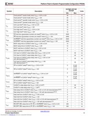
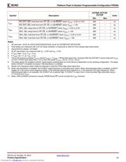
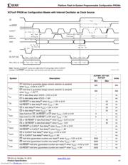
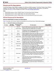
Pinouts and Pin Descriptions
The XCFxxS Platform Flash PROM is available in the VO20 and VOG20 packages. The XCFxxP Platform Flash PROM is
available in the VO48, VOG48, FS48, and FSG48 packages. For package drawings, specifications, and additional
information, see UG112
, Device Package User Guide, or the Xilinx Package Specifications.
Note:
1. VO20/VOG20 denotes a 20-pin (TSSOP) Plastic Thin Shrink Small Outline Package.
2. VO48/VOG48 denotes a 48-pin (TSOP) Plastic Thin Small Outline Package.
3. FS48/FSG48 denotes a 48-pin (TFBGA) Plastic Thin Fine Pitch Ball Grid Array (0.8 mm pitch).
XCFxxS Pinouts and Pin Descriptions
XCFxxS VO20/VOG20 Pin Names and Descriptions
Tabl e 1 2 provides a list of the pin names and descriptions for the XCFxxS 20-pin VO20/VOG20 package.
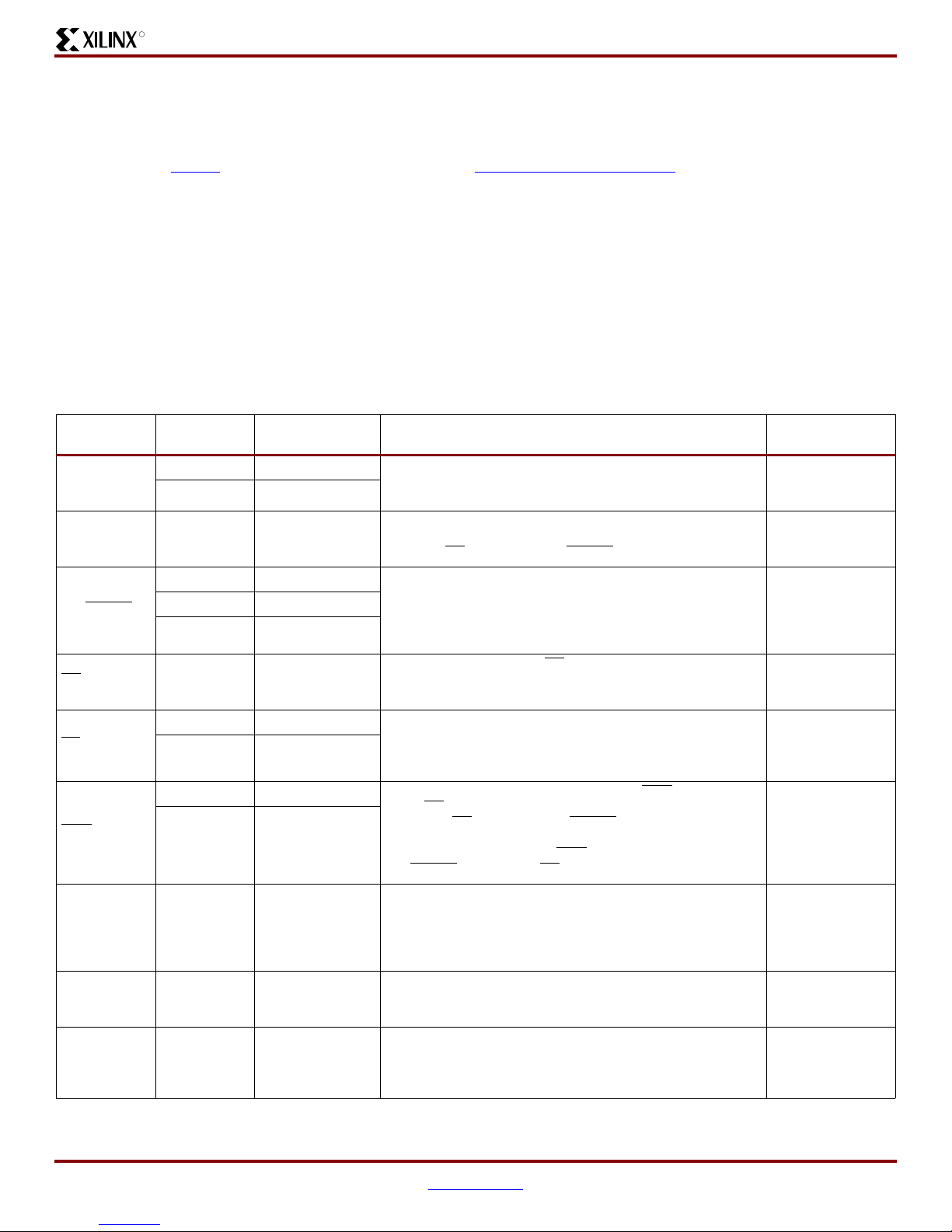
Tabl e 12 : XCFxxS Pin Names and Descriptions
Pin Name
Boundary
Scan Order
Boundary-Scan
Function
Pin Description
20-pin TSSOP
(VO20/VOG20)
D0
4 Data Out D0 is the DATA output pin to provide data for configuring an
FPGA in serial mode. The D0 output is set to a high-
impedance state during ISPEN (when not clamped).
1
3 Output Enable
CLK 0 Data In
Configuration Clock Input. Each rising edge on the CLK input
increments the internal address counter if the CLK input is
selected, CE
is Low, and OE/RESET is High.
3
OE/RESET
20 Data In Output Enable/Reset (Open-Drain I/O). When Low, this input
holds the address counter reset and the DATA output is in a
high-impedance state. This is a bidirectional open-drain pin
that is held Low while the PROM completes the internal
power-on reset sequence. Polarity is not programmable.
8
19 Data Out
18 Output Enable
CE
15 Data In
Chip Enable Input. When CE
is High, the device is put into
low-power standby mode, the address counter is reset, and
the DATA pins are put in a high-impedance state.
10
CF
22 Data Out Configuration Pulse (Open-Drain Output). Allows JTAG
CONFIG instruction to initiate FPGA configuration without
powering down FPGA. This is an open-drain output that is
pulsed Low by the JTAG CONFIG command.
7
21 Output Enable
CEO
12 Data Out Chip Enable Output. Chip Enable Output (CEO) is connected
to the CE
input of the next PROM in the chain. This output is
Low when CE
is Low and OE/RESET input is High, AND the
internal address counter has been incremented beyond its
Terminal Count (TC) value. CEO
returns to High when
OE/RESET
goes Low or CE goes High.
13
11 Output Enable
TMS – Mode Select
JTAG Mode Select Input. The state of TMS on the rising edge
of TCK determines the state transitions at the Test Access
Port (TAP) controller. TMS has an internal 50 kΩ resistive pull-
up to V
CCJ
to provide a logic 1 to the device if the pin is not
driven.
5
TCK – Clock
JTAG Clock Input. This pin is the JTAG test clock. It
sequences the TAP controller and all the JTAG test and
programming electronics.
6
TDI – Data In
JTAG Serial Data Input. This pin is the serial input to all JTAG
instruction and data registers. TDI has an internal 50 kΩ
resistive pull-up to V
CCJ
to provide a logic 1 to the device if the
pin is not driven.
4
Downloaded from Elcodis.com electronic components distributor
器件 Datasheet 文档搜索
AiEMA 数据库涵盖高达 72,405,303 个元件的数据手册,每天更新 5,000 多个 PDF 文件
