Datasheet 搜索 > FPGA芯片 > Altera(阿尔特拉) > 5CSEBA6U23C7N 数据手册 > 5CSEBA6U23C7N 其他数据使用手册 3/169 页

¥ 1508.85
5CSEBA6U23C7N 其他数据使用手册 - Altera(阿尔特拉)
制造商:
Altera(阿尔特拉)
分类:
FPGA芯片
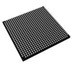
封装:
UBGA-672
Pictures:
3D模型
符号图
焊盘图
引脚图
产品图
页面导航:
原理图在P12P13P15P22P27P33
技术参数、封装参数在P132
应用领域在P164
导航目录
5CSEBA6U23C7N数据手册
Page:
of 169 Go
若手册格式错乱,请下载阅览PDF原文件

Resetting the Transmitter with the User-Coded Reset Controller During Device Power-
Up ................................................................................................................................................ 3-7
Resetting the Transmitter with the User-Coded Reset Controller During Device
Operation.....................................................................................................................................3-8
Resetting the Receiver with the User-Coded Reset Controller During Device Power-Up
Configuration..............................................................................................................................3-9
Resetting the Receiver with the User-Coded Reset Controller During Device Operation
.....................................................................................................................................................3-10
Transceiver Reset Using Avalon Memory Map Registers....................................................................3-11
Transceiver Reset Control Signals Using Avalon Memory Map Registers............................3-11
Clock Data Recovery in Manual Lock Mode......................................................................................... 3-12
Control Settings for CDR Manual Lock Mode..........................................................................3-13
Resetting the Transceiver in CDR Manual Lock Mode............................................................3-13
Resetting the Transceiver During Dynamic Reconfiguration.............................................................3-14
Guidelines for Dynamic Reconfiguration if Transmitter Duty Cycle Distortion
Calibration is Required During Device Operation..............................................................3-14
Transceiver Blocks Affected by the Reset and Powerdown Signals....................................................3-15
Transceiver Power-Down.........................................................................................................................3-16
Document Revision History.....................................................................................................................3-16
Transceiver Protocol Configurations in Cyclone V Devices..............................4-1
PCI Express...................................................................................................................................................4-2
PCIe Transceiver Datapath.............................................................................................................4-3
PCIe Supported Features................................................................................................................ 4-4
PCIe Supported Configurations and Placement Guidelines......................................................4-7
Gigabit Ethernet.........................................................................................................................................4-13
Gigabit Ethernet Transceiver Datapath......................................................................................4-15
XAUI............................................................................................................................................................4-19
Transceiver Datapath in a XAUI Configuration.......................................................................4-19
XAUI Supported Features............................................................................................................ 4-21
Transceiver Clocking and Channel Placement Guidelines in XAUI Configuration........... 4-24
Serial Digital Interface...............................................................................................................................4-26
Configurations Supported in SDI Mode.....................................................................................4-27
Serial Digital Interface Transceiver Datapath............................................................................4-29
Serial Data Converter (SDC) JESD204................................................................................................... 4-30
SATA and SAS Protocols..........................................................................................................................4-31
Deterministic Latency Protocols—CPRI and OBSAI...........................................................................4-32
Latency Uncertainty Removal with the Phase Compensation FIFO in Register Mode.......4-33
Channel PLL Feedback for Deterministic Relationship...........................................................4-33
CPRI and OBSAI............................................................................................................................4-33
6.144-Gbps Support Capability in Cyclone V GT Devices...................................................... 4-35
CPRI Enhancements......................................................................................................................4-37
Document Revision History.....................................................................................................................4-38
Transceiver Custom Configurations in Cyclone V Devices...............................5-1
Standard PCS Configuration......................................................................................................................5-1
Custom Configuration Channel Options.....................................................................................5-2
Cyclone V Device Handbook Volume 2: Transceivers
TOC-3
Altera Corporation
器件 Datasheet 文档搜索
AiEMA 数据库涵盖高达 72,405,303 个元件的数据手册,每天更新 5,000 多个 PDF 文件
