Datasheet 搜索 > FPGA芯片 > Altera(阿尔特拉) > 5CSEBA6U23C7N 数据手册 > 5CSEBA6U23C7N 其他数据使用手册 6/169 页

¥ 1508.85
5CSEBA6U23C7N 其他数据使用手册 - Altera(阿尔特拉)
制造商:
Altera(阿尔特拉)
分类:
FPGA芯片
封装:
UBGA-672
Pictures:
3D模型
符号图
焊盘图
引脚图
产品图
页面导航:
原理图在P12P13P15P22P27P33
技术参数、封装参数在P132
应用领域在P164
导航目录
5CSEBA6U23C7N数据手册
Page:
of 169 Go
若手册格式错乱,请下载阅览PDF原文件
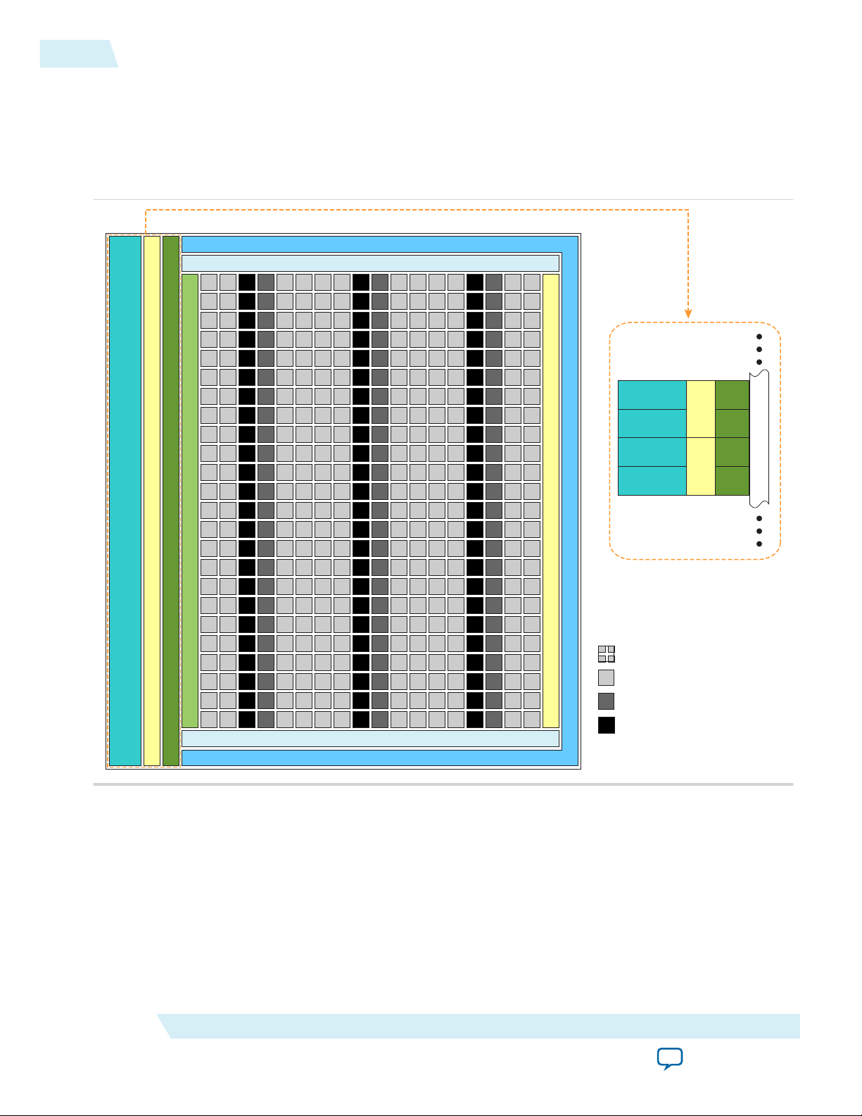
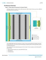
Architecture Overview
Figure 1-1: Basic Layout of Transceivers in a Cyclone V Device
This figure represents a Cyclone V device with transceivers. Other Cyclone V devices may have a different
floor plan than the one shown here.
I/O, LVDS, and Memory Interface
I/O, LVDS, and Memory Interface
I/O, LVDS, and Memory Interface
Transceiver Channels
Fractional PLLs
Hard PCS Blocks
Fractional
PLL
Fractional
PLL
Fractional PLLs
PCIe Hard IP Blocks
Hard Memory Controller
Hard Memory Controller
Core Logic Fabric and MLABs
Variable-Precision DSP Blocks
M10K Internal Memory Blocks
Distributed Memory
Transceiver
PMA
Hard
PCS
Transceiver
PMA
Hard
PCS
Transceiver
PMA
Hard
PCS
Transceiver
PMA
Hard
PCS
Clock Networks
Transceiver
Individual Channels
The embedded high-speed clock networks in Cyclone V devices provide dedicated clocking connectivity
for the transceivers. You can also use the fractional phase-locked loop (fPLL) between the PMA and PCS
to clock the transceivers.
The embedded PCIe hard intellectual property (IP) of Cyclone V devices implements the following PCIe
protocol stacks:
• Physical interface/media access control (PHY/MAC) layer
• Data link layer
• Transaction layer
1-2
Architecture Overview
CV-53001
2016.01.28
Altera Corporation
Transceiver Architecture in Cyclone V Devices
Send Feedback
器件 Datasheet 文档搜索
AiEMA 数据库涵盖高达 72,405,303 个元件的数据手册,每天更新 5,000 多个 PDF 文件
