Datasheet 搜索 > DA转换器 > ADI(亚德诺) > AD5693BCPZ-RL7 数据手册 > AD5693BCPZ-RL7 其他数据使用手册 1/27 页
 器件3D模型
¥ 13.453
AD5693BCPZ-RL7 其他数据使用手册 - ADI(亚德诺)
制造商:
ADI(亚德诺)
分类:
DA转换器
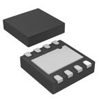
封装:
LFCSP-8
Pictures:
3D模型
符号图
焊盘图
引脚图
产品图
页面导航:
引脚图在P8P9P10P11P20P25Hot
原理图在P1P19
封装尺寸在P25
型号编码规则在P26
功能描述在P1P8P9P10P11P25
技术参数、封装参数在P1P3P7
应用领域在P1
电气规格在P12
导航目录
AD5693BCPZ-RL7数据手册
Page:
of 27 Go
若手册格式错乱,请下载阅览PDF原文件
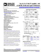
Tiny 16-/14-/12-Bit I
2
C nanoDAC+, with
±2 LSB INL (16-Bit) and 2 ppm/°C Reference
Data Sheet
AD5693R/AD5692R/AD5691R/AD5693
Rev. D Document Feedback
Information furnished by Analog Devices is believed to be accurate and reliable. However, no
responsibility is assumed by Analog Devices for its use, nor for any infringements of patents or other
rights of third parties that may result from its use. Specifications subject to change without notice. No
license is granted by implication or otherwise under any patent or patent rights of Analog Devices.
Trademarks and registered trademarks are the property of their respective owners.
One Technology Way, P.O. Box 9106, Norwood, MA 02062-9106, U.S.A.
Tel: 781.329.4700 ©2014–2017 Analog Devices, Inc. All rights reserved.
Technical Support www.analog.com
FEATURES
Ultrasmall package: 2 mm × 2 mm, 8-lead LFCSP
High relative accuracy (INL): ±2 LSB maximum at 16 bits
AD5693R/AD5692R/AD5691R
Low drift, 2.5 V reference: 2 ppm/°C typical
Selectable span output: 2.5 V or 5 V
AD5693
External reference only
Selectable span output: V
REF
or 2 × V
REF
Total unadjusted error (TUE): ±0.06% of FSR maximum
Offset error: ±1.5 mV maximum
Gain error: ±0.05 % of FSR maximum
Low glitch: 0.1 nV-sec
High drive capability: 20 mA
Low power: 1.2 mW at 3.3 V
1.8 V V
LOGIC
compatible
Wide operating temperature range: −40°C to +105°C
APPLICATIONS
Process controls
Data acquisition systems
Digital gain and offset adjustment
Programmable voltage sources
Optical modules
GENERAL DESCRIPTION
The AD5693R/AD5692R/AD5691R/AD5693, members of the
nanoDAC+® family, are low power, single-channel, 16-/14-/12-bit
buffered voltage output DACs. The devices, except the AD5693,
include an enabled by default internal 2.5 V reference, offering
2 ppm/°C drift. The output span can be programmed to be 0 V to
V
REF
or 0 V to 2 × V
REF
. All devices operate from a single 2.7 V to
5.5 V supply and are guaranteed monotonic by design. The
devices are available in a 2.00 mm × 2.00 mm, 8-lead LFCSP or
a 10-lead MSOP.
The internal power-on reset circuit ensures that the DAC register
is written to zero scale at power-up while the internal output
buffer is configured in normal mode. The AD5693R/AD5692R/
AD5691R/AD5693 contain a power-down mode that reduces the
current consumption of the device to 2 µA (maximum) at 5 V and
provides software selectable output loads.
The AD5693R/AD5692R/AD5691R/AD5693 use an I
2
C
interface. Some device options also include an asynchronous
RESET
pin and a V
LOGIC
pin, allowing 1.8 V compatibility.
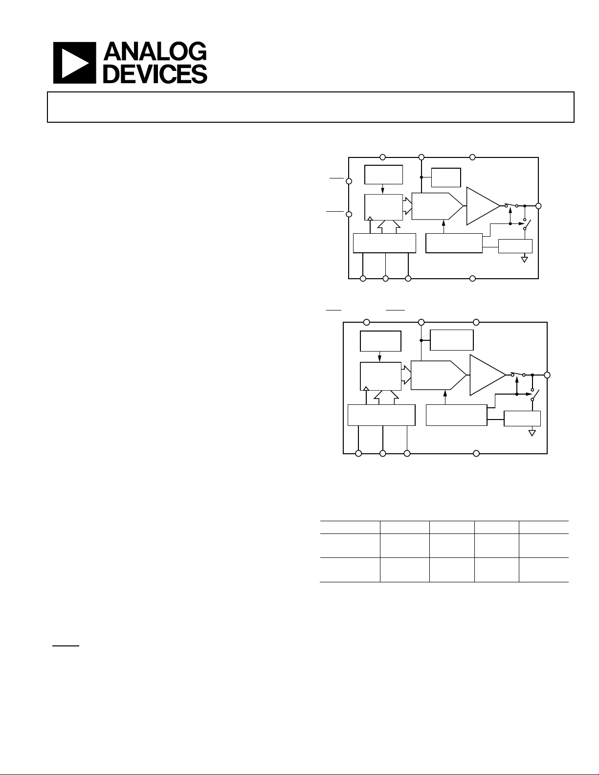
FUNCTIONAL BLOCK DIAGRAM
AD5693R/
AD5692R/
AD5691R
V
REF
GND
LDAC
REF
V
DD
V
LOGIC
POWER-DOWN
CONTROL LOGIC
DAC
REGISTER
POWER-ON
RESET
2.5V
REF
OUTPUT
BUFFER
16-/14-/12-BIT
DAC
INPUT
CONTROL LOGIC
V
OUT
SCL
SDA
RESET
A0
RESISTOR
NETWORK
12077-001
Figure 1. MSOP
12077-002
AD5693R/
AD5692R/
AD5691R/
AD5693
V
REF
GND
REF
V
DD
LDAC OR V
LOGIC
OR RESET
1
POWER-DOWN
CONTROL LOGIC
DAC
REGISTER
POWER-ON
RESET
2.5V REF
2
OUTPUT
BUFFER
16-/14-/12-BIT
DAC
INPUT
CONTROL LOGIC
V
OUT
SCLSDA A0
RESISTOR
NETWORK
1
NOT ALL PINS AVAILABLE IN ALL 8-LEAD LFCSP MODELS.
2
NOT AVAILABLE IN THE AD5693.
Figure 2. LFCSP
Table 1. Related Devices
Interface
Reference
16-Bit
14-Bit
12-Bit
SPI
Internal
AD5683R
AD5682R
AD5681R
External
AD5683
I
2
C Internal AD5693R AD5692R AD5691R
External AD5693
PRODUCT HIGHLIGHTS
1. High relative accuracy (INL): ±2 LSB maximum
(AD5693R/AD5693, 16-bit).
2. Low drift, 2.5 V on-chip reference: 2 ppm/°C typical and
5 ppm/°C maximum temperature coefficient.
3. 2 mm × 2 mm, 8-lead LFCSP and 10-lead MSOP.
器件 Datasheet 文档搜索
AiEMA 数据库涵盖高达 72,405,303 个元件的数据手册,每天更新 5,000 多个 PDF 文件
