Datasheet 搜索 > MOS管 > NXP(恩智浦) > BUK7535-100A127 数据手册 > BUK7535-100A127 其他数据使用手册 6/14 页

¥ 3.269
BUK7535-100A127 其他数据使用手册 - NXP(恩智浦)
制造商:
NXP(恩智浦)
分类:
MOS管
Pictures:
3D模型
符号图
焊盘图
引脚图
产品图
页面导航:
导航目录
BUK7535-100A127数据手册
Page:
of 14 Go
若手册格式错乱,请下载阅览PDF原文件

BUK7535-100A All information provided in this document is subject to legal disclaimers. © NXP B.V. 2011. All rights reserved.
Product data sheet Rev. 02 — 21 February 2011 6 of 14
NXP Semiconductors
BUK7535-100A
N-channel TrenchMOS standard level FET
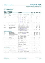
6. Characteristics
Table 6. Characteristics
Symbol Parameter Conditions Min Typ Max Unit
Static characteristics
V
(BR)DSS
drain-source breakdown
voltage
I
D
=0.25mA; V
GS
=0V; T
j
= 25 °C 100 - - V
I
D
=0.25mA; V
GS
=0V; T
j
= -55 °C 89 - - V
V
GS(th)
gate-source threshold voltage I
D
=1mA; V
DS
=V
GS
; T
j
=25°C;
see Figure 11
234V
I
D
=1mA; V
DS
=V
GS
; T
j
=-55°C;
see Figure 11
--4.4V
I
D
=1mA; V
DS
=V
GS
; T
j
= 175 °C;
see Figure 11
1--V
I
DSS
drain leakage current V
DS
=100V; V
GS
=0V; T
j
= 25 °C - 0.05 10 µA
V
DS
=100V; V
GS
=0V; T
j
= 175 °C - - 500 µA
I
GSS
gate leakage current V
GS
=20V; V
DS
=0V; T
j
= 25 °C - 2 100 nA
V
GS
=-20V; V
DS
=0V; T
j
= 25 °C - 2 100 nA
R
DSon
drain-source on-state
resistance
V
GS
=10V; I
D
=25A; T
j
= 175 °C;
see Figure 12; see Figure 13
--88mΩ
V
GS
=10V; I
D
=25A; T
j
=25°C;
see Figure 12
; see Figure 13
- 2135mΩ
Dynamic characteristics
C
iss
input capacitance V
GS
=0V; V
DS
=25V; f=1MHz;
T
j
=25°C; see Figure 14
- 1900 2535 pF
C
oss
output capacitance - 250 301 pF
C
rss
reverse transfer capacitance - 150 205 pF
t
d(on)
turn-on delay time V
DS
=30V; R
L
=1.2Ω; V
GS
=10V;
R
G(ext)
=10Ω; T
j
=25°C
-15-ns
t
r
rise time V
DS
=30V; V
GS
=10V;
R
G(ext)
=10Ω
-67-ns
t
d(off)
turn-off delay time - 56 - ns
t
f
fall time V
DS
=30V; R
L
=1.2Ω; V
GS
=10V;
R
G(ext)
=10Ω
-35-ns
L
D
internal drain inductance from contact screw on mounting base
to centre of die ; T
j
=25°C
-3.5-nH
from drain lead 6 mm from package to
centre of die ; T
j
=25°C
-4.5-nH
L
S
internal source inductance from source lead to source bond pad ;
T
j
=25°C
-7.5-nH
Source-drain diode
V
SD
source-drain voltage I
S
=25A; V
GS
=0V; T
j
=25°C;
see Figure 15
- 0.85 1.2 V
t
rr
reverse recovery time I
S
=20A; dI
S
/dt = -100 A/µs;
V
GS
=-10V; V
DS
=30V; T
j
=25°C
-67-ns
Q
r
recovered charge - 220 - nC
器件 Datasheet 文档搜索
AiEMA 数据库涵盖高达 72,405,303 个元件的数据手册,每天更新 5,000 多个 PDF 文件
