Datasheet 搜索 > EEPROM芯片 > ON Semiconductor(安森美) > CAV24C128YE-GT3 数据手册 > CAV24C128YE-GT3 其他数据使用手册 1/12 页
 器件3D模型
¥ 1.395
CAV24C128YE-GT3 其他数据使用手册 - ON Semiconductor(安森美)
制造商:
ON Semiconductor(安森美)
分类:
EEPROM芯片
封装:
TSSOP-8
描述:
CAV24C128: EEPROM 串行 128-Kb I2C - 汽车级
Pictures:
3D模型
符号图
焊盘图
引脚图
产品图
页面导航:
导航目录
CAV24C128YE-GT3数据手册
Page:
of 12 Go
若手册格式错乱,请下载阅览PDF原文件
© Semiconductor Components Industries, LLC, 2012
April, 2019 − Rev. 2
1 Publication Order Number:
CAV24C128/D
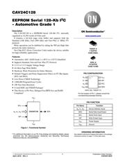
CAV24C128
EEPROM Serial 128-Kb I
2
C
- Automotive Grade 1
Description
The CAV24C128 is a EEPROM Serial 128−Kb I
2
C, internally
organized as 16,384 words of 8 bits each.
It features a 64−byte page write buffer and supports both the
Standard (100 kHz), Fast (400 kHz) and Fast−Plus (1 MHz) I
2
C
protocol.
Write operations can be inhibited by taking the WP pin High (this
protects the entire memory).
On−Chip ECC (Error Correction Code) makes the device suitable
for high reliability applications.
Features
• Automotive AEC−Q100 Grade 1 (−40°C to +125°C) Qualified
• Supports Standard, Fast and Fast−Plus I
2
C Protocol
• 2.5 V to 5.5 V Supply Voltage Range
• 64−Byte Page Write Buffer
• Hardware Write Protection for Entire Memory
• Schmitt Triggers and Noise Suppression Filters on I
2
C Bus Inputs
(SCL and SDA)
• Low Power CMOS Technology
• 1,000,000 Program/Erase Cycles
• 100 Year Data Retention
• 8−lead SOIC and TSSOP Packages
• This Device is Pb−Free, Halogen Free/BFR Free and RoHS
Compliant*
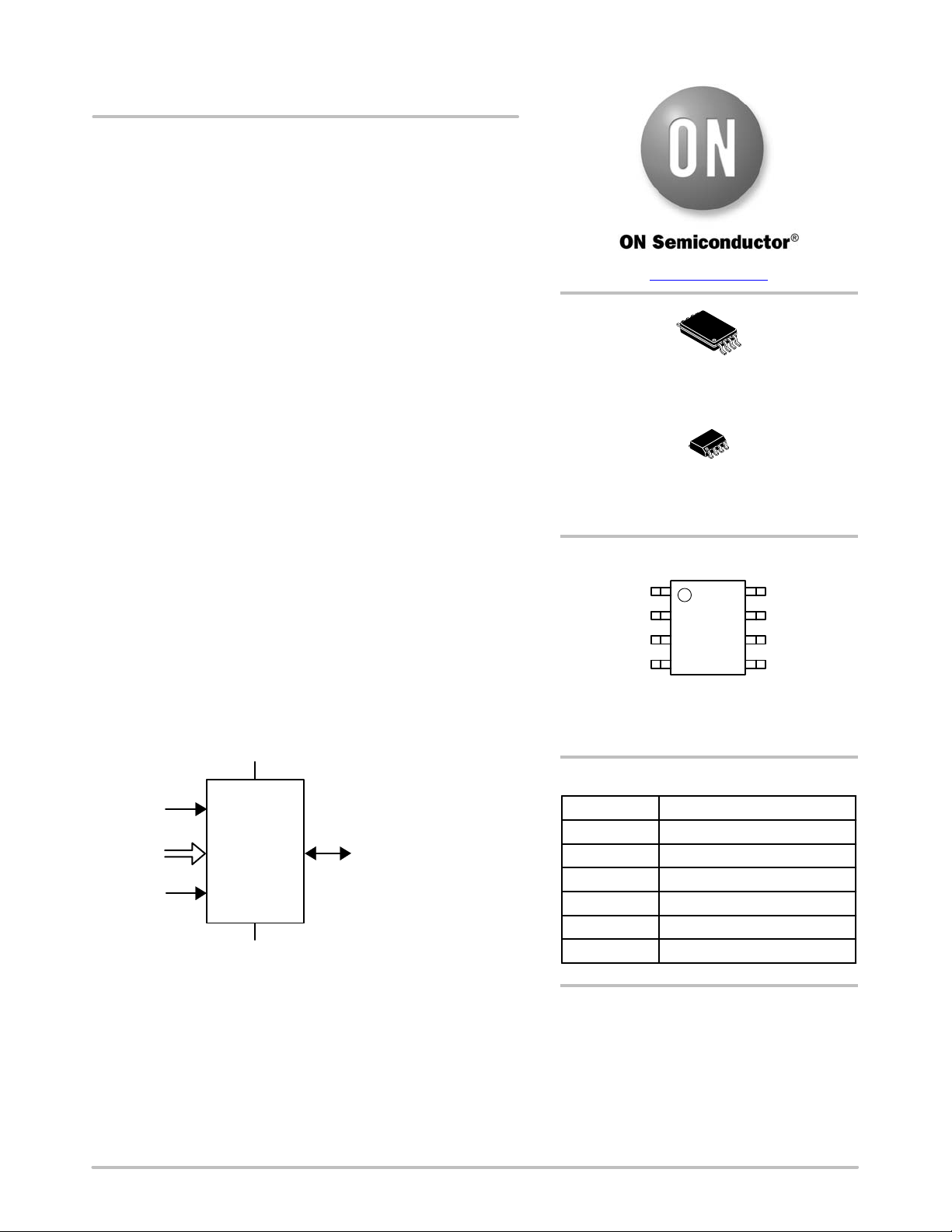
Figure 1. Functional Symbol
SDA
SCL
WP
CAV24C128
V
CC
V
SS
A
2
, A
1
, A
0
* For additional information on our Pb−Free strategy and soldering details, please
download the ON Semiconductor Soldering and Mounting Techniques
Reference Manual, SOLDERRM/D.
www.onsemi.com
PIN CONFIGURATION
See detailed ordering and shipping information in the package
dimensions section on page 11 of this data sheet.
ORDERING INFORMATION
SOIC−8
W SUFFIX
CASE 751BD
SOIC (W), TSSOP (Y)
TSSOP−8
Y SUFFIX
CASE 948AL
Device Address InputsA
0
, A
1
, A
2
Serial Data Input/OutputSDA
Serial Clock InputSCL
Write Protect InputWP
Power SupplyV
CC
GroundV
SS
FunctionPin Name
PIN FUNCTION
For the location of Pin 1, please consult the
corresponding package drawing.
SDA
WP
V
CC
V
SS
A
2
A
1
A
0
1
SCL
器件 Datasheet 文档搜索
AiEMA 数据库涵盖高达 72,405,303 个元件的数据手册,每天更新 5,000 多个 PDF 文件
