Datasheet 搜索 > EEPROM芯片 > ON Semiconductor(安森美) > CAV24C128YE-GT3 数据手册 > CAV24C128YE-GT3 其他数据使用手册 2/12 页
 器件3D模型
¥ 1.394
CAV24C128YE-GT3 其他数据使用手册 - ON Semiconductor(安森美)
制造商:
ON Semiconductor(安森美)
分类:
EEPROM芯片
封装:
TSSOP-8
描述:
CAV24C128: EEPROM 串行 128-Kb I2C - 汽车级
Pictures:
3D模型
符号图
焊盘图
引脚图
产品图
页面导航:
导航目录
CAV24C128YE-GT3数据手册
Page:
of 12 Go
若手册格式错乱,请下载阅览PDF原文件
CAV24C128
www.onsemi.com
2
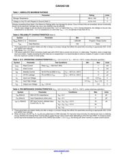
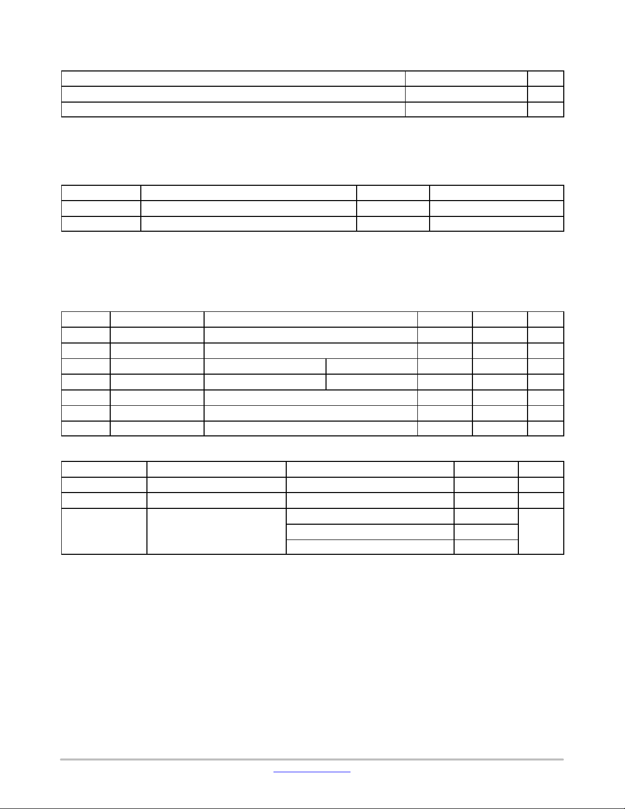
Table 1. ABSOLUTE MAXIMUM RATINGS
Parameter Rating Units
Storage Temperature −65 to +150 °C
Voltage on Any Pin with Respect to Ground (Note 1) −0.5 to +6.5 V
Stresses exceeding those listed in the Maximum Ratings table may damage the device. If any of these limits are exceeded, device functionality
should not be assumed, damage may occur and reliability may be affected.
1. The DC input voltage on any pin should not be lower than −0.5 V or higher than V
CC
+ 0.5 V. During transitions, the voltage on any pin may
undershoot to no less than −1.5 V or overshoot to no more than V
CC
+ 1.5 V, for periods of less than 20 ns.
Table 2. RELIABILITY CHARACTERISTICS (Note 2)
Symbol Parameter Min Units
N
END
(Notes 3, 4) Endurance 1,000,000 Program / Erase Cycles
T
DR
Data Retention 100 Years
2. These parameters are tested initially and after a design or process change that affects the parameter according to appropriate AEC−Q100
and JEDEC test methods.
3. Page Mode, V
CC
= 5 V, 25°C
4. This device uses ECC (Error Correction Code) logic with 6 ECC bits to correct one bit error in 4 data bytes. Therefore, when a single byte
has to be written, 4 bytes (including the ECC bits) are re−programmed. It is recommended to write by multiple of 4 bytes in order to benefit
from the maximum number of write cycles.
Table 3. D.C. OPERATING CHARACTERISTICS (V
CC
= 2.5 V to 5.5 V, T
A
= −40°C to +125°C, unless otherwise specified.)
Symbol
Parameter Test Conditions Min Max Units
I
CCR
Read Current Read, f
SCL
= 400 kHz/1 MHz 1 mA
I
CCW
Write Current 3 mA
I
SB
Standby Current All I/O Pins at GND or V
CC
T
A
= −40°C to +125°C 5
mA
I
L
I/O Pin Leakage Pin at GND or V
CC
T
A
= −40°C to +125°C 2
mA
V
IL
Input Low Voltage −0.5 0.3 V
CC
V
V
IH
Input High Voltage 0.7 V
CC
V
CC
+ 0.5 V
V
OL
Output Low Voltage I
OL
= 3.0 mA 0.4 V
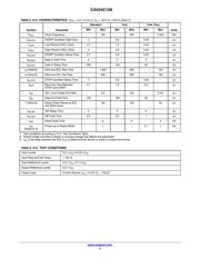
Table 4. PIN IMPEDANCE CHARACTERISTICS (V
CC
= 2.5 V to 5.5 V, T
A
= −40°C to +125°C, unless otherwise specified.)
Symbol Parameter Conditions Max Units
C
IN
(Note 5) SDA I/O Pin Capacitance V
IN
= 0 V 8 pF
C
IN
(Note 5) Input Capacitance (other pins) V
IN
= 0 V 6 pF
I
WP
, I
A
(Note 6) WP Input Current, Address Input
Current (A
0
, A
1
, A
2
)
V
IN
< V
IH
, V
CC
= 5.5 V 75 mA
V
IN
< V
IH
, V
CC
= 3.3 V 50
V
IN
> V
IH
2
5. These parameters are tested initially and after a design or process change that affects the parameter according to appropriate AEC−Q100
and JEDEC test methods.
6. When not driven, the WP, A
0
, A
1
, A
2
pins are pulled down to GND internally. For improved noise immunity, the internal pull−down is relatively
strong; therefore the external driver must be able to supply the pull−down current when attempting to drive the input HIGH. To conserve power,
as the input level exceeds the trip point of the CMOS input buffer (~ 0.5 x V
CC
), the strong pull−down reverts to a weak current source.
器件 Datasheet 文档搜索
AiEMA 数据库涵盖高达 72,405,303 个元件的数据手册,每天更新 5,000 多个 PDF 文件
