Datasheet 搜索 > MOS管 > Fairchild(飞兆/仙童) > FDMC86520DC 数据手册 > FDMC86520DC 其他数据使用手册 1/9 页


¥ 6.274
FDMC86520DC 其他数据使用手册 - Fairchild(飞兆/仙童)
制造商:
Fairchild(飞兆/仙童)
分类:
MOS管
封装:
DualCool-33-8
描述:
PowerTrench® N 通道 MOSFET,10A 至 19.9A,Fairchild Semiconductor### MOSFET 晶体管,Fairchild SemiconductorFairchild 提供大量 MOSFET 设备组合,包括高电压 (>250V) 低电压 (Fairchild MOSFET 通过降低电压峰值和过冲提供极佳的设计可靠性,以减少结电容和反向恢复电荷,无需额外外部元件即可保持系统启动和运行更长时间。
Pictures:
3D模型
符号图
焊盘图
引脚图
产品图

FDMC86520DC数据手册
Page:
of 9 Go
若手册格式错乱,请下载阅览PDF原文件
February 2016
©2012 Fairchild Semiconductor Corporation
FDMC8588DC Rev.1.1
www.fairchildsemi.com
1
FDMC8588DC N-Channel Dual Cool
TM
33 PowerTrench
®
MOSFET
FDMC8588DC
N-Channel Dual Cool
TM
33 PowerTrench
®
MOSFET
25 V, 40 A, 5.7 mΩ
Features
Dual Cool
TM
Top Side Cooling PQFN package
Max r
DS(on)
= 5.7 mΩ at V
GS
= 4.5 V, I
D
= 17 A
State-of-the-art switching performance
Lower output capacitance, gate resistance, and gate charge
boost efficiency
Shielded gate technology reduces switch node ringing and
increases immunity to EMI and cross conduction
RoHS Compliant
General Description
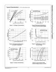
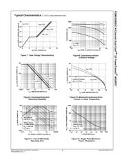
This N-Channel MOSFET has been designed specifically to
improve the overall efficiency and to minimize switch node
ringing of DC/DC converters using either synchronous or
conventional switching PWM controllers. It has been optimized
for low gate charge, low r
DS(on)
, fast switching speed and body
diode reverse recovery performance.
Applications
High side switching for high end computing
High power density DC-DC synchronous buck converter
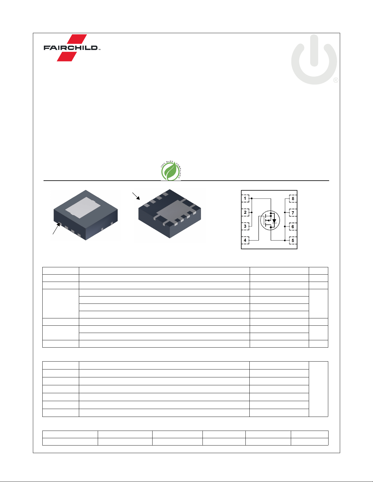
Top
Dual Cool
TM
33
Bottom
D
D
D
D
G
S
S
S
Pin 1
Pin 1
S
S
S
G
D
D
D
D
MOSFET Maximum Ratings T
A
= 25 °C unless otherwise noted
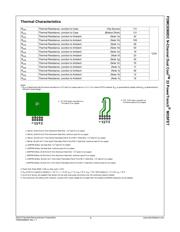
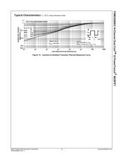
Thermal Characteristics
Package Marking and Ordering Information
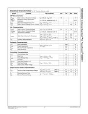
Symbol Parameter Ratings Units
V
DS
Drain to Source Voltage (Note 5) 25 V
V
GS
Gate to Source Voltage (Note 4) ±12 V
I
D
Drain Current - Continuous (Package limited) T
C
= 25 °C 40
A
- Continuous (Silicon Limited) T
C
= 25 °C 73
- Continuous (Note 1a) 17
- Pulsed 60
E
AS
Single Pulse Avalanche Energy (Note 3) 29 mJ
P
D
Power Dissipation T
C
= 25 °C 41
W
Power Dissipation T
A
= 25 °C (Note 1a) 3.0
T
J
, T
STG
Operating and Storage Junction Temperature Range -55 to +150 °C
R
θJC
Thermal Resistance, Junction to Case (Top Source) 7.0
°C/W
R
θJC
Thermal Resistance, Junction to Case (Bottom Drain) 3.0
R
θJA
Thermal Resistance, Junction to Ambient (Note 1a) 42
R
θJA
Thermal Resistance, Junction to Ambient (Note 1b) 105
R
θJA
Thermal Resistance, Junction to Ambient (Note 1i) 17
R
θJA
Thermal Resistance, Junction to Ambient (Note 1j) 26
R
θJA
Thermal Resistance, Junction to Ambient (Note 1k) 12
Device Marking Device Package Reel Size Tape Width Quantity
08DC FDMC8588DC
Dual Cool
TM
33
13 ’’ 12 mm 3000 units
器件 Datasheet 文档搜索
AiEMA 数据库涵盖高达 72,405,303 个元件的数据手册,每天更新 5,000 多个 PDF 文件
