Datasheet 搜索 > 仪表放大器 > TI(德州仪器) > INA333AIDGKR 数据手册 > INA333AIDGKR 其他数据使用手册 1/34 页
 器件3D模型
¥ 3.603
INA333AIDGKR 其他数据使用手册 - TI(德州仪器)
制造商:
TI(德州仪器)
分类:
仪表放大器
封装:
VSSOP-8
描述:
TEXAS INSTRUMENTS INA333AIDGKR 仪器放大器, 1个放大器, 10 µV, 0.16 V/µs, 150 kHz, 1.8V 至 5.5V, VSSOP
Pictures:
3D模型
符号图
焊盘图
引脚图
产品图
页面导航:
引脚图在P3Hot
典型应用电路图在P14P15
原理图在P1P13
封装尺寸在P24P26P27
标记信息在P24
封装信息在P23P24P25P26P27
技术参数、封装参数在P4
应用领域在P1
电气规格在P5P6
导航目录
INA333AIDGKR数据手册
Page:
of 34 Go
若手册格式错乱,请下载阅览PDF原文件
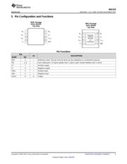
50kW
150kW 150kW
A
1
A
3
V
OUT
V
IN-
6
REF
5
RFIFilteredInputs
2
V+
7
V-
4
1
8
150kW 150kW
50kW
A
2
V
IN+
RFIFilteredInputs
3
INA333
R
G
G=1+
100kW
R
G
RFIFilteredInputs
RFIFilteredInputs
Product
Folder
Sample &
Buy
Technical
Documents
Tools &
Software
Support &
Community
An IMPORTANT NOTICE at the end of this data sheet addresses availability, warranty, changes, use in safety-critical applications,
intellectual property matters and other important disclaimers. PRODUCTION DATA.
INA333
SBOS445C –JULY 2008–REVISED DECEMBER 2015
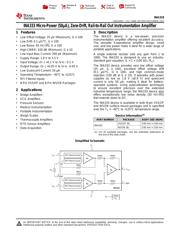
INA333 Micro-Power (50μA), Zerø-Drift, Rail-to-Rail Out Instrumentation Amplifier
1
1 Features
1
• Low Offset Voltage: 25 μV (Maximum), G ≥ 100
• Low Drift: 0.1 μV/°C, G ≥ 100
• Low Noise: 50 nV/√Hz, G ≥ 100
• High CMRR: 100 dB (Minimum), G ≥ 10
• Low Input Bias Current: 200 pA (Maximum)
• Supply Range: 1.8 V to 5.5 V
• Input Voltage: (V–) +0.1 V to (V+) –0.1 V
• Output Range: (V–) +0.05 V to (V+) –0.05 V
• Low Quiescent Current: 50 μA
• Operating Temperature: –40°C to +125°C
• RFI Filtered Inputs
• 8-Pin VSSOP and 8-Pin WSON Packages
2 Applications
• Bridge Amplifiers
• ECG Amplifiers
• Pressure Sensors
• Medical Instrumentation
• Portable Instrumentation
• Weigh Scales
• Thermocouple Amplifiers
• RTD Sensor Amplifiers
• Data Acquisition
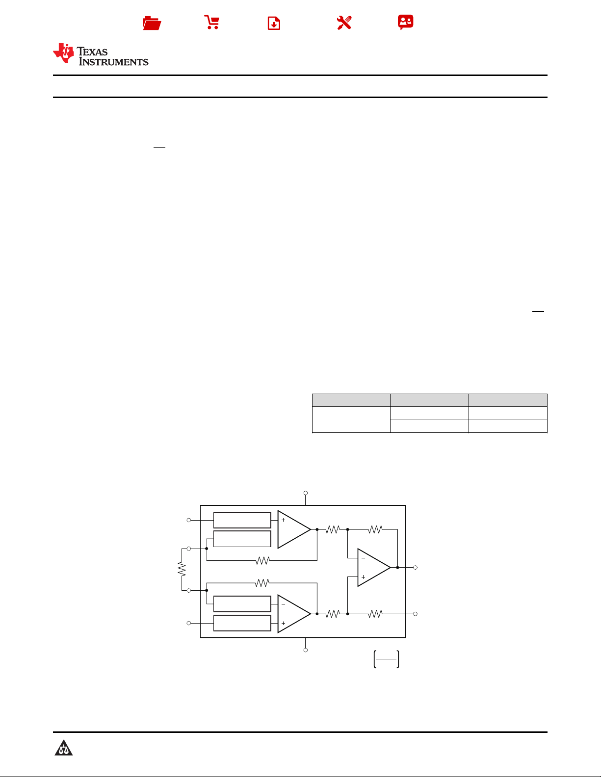
3 Description
The INA333 device is a low-power, precision
instrumentation amplifier offering excellent accuracy.
The versatile 3-operational amplifier design, small
size, and low power make it ideal for a wide range of
portable applications.
A single external resistor sets any gain from 1 to
1000. The INA333 is designed to use an industry-
standard gain equation: G = 1 + (100 kΩ / R
G
).
The INA333 device provides very low offset voltage
(25 μV, G ≥ 100), excellent offset voltage drift
(0.1 μV/°C, G ≥ 100), and high common-mode
rejection (100 dB at G ≥ 10). It operates with power
supplies as low as 1.8 V (±0.9 V) and quiescent
current is only 50 μA, making it ideal for battery-
operated systems. Using autocalibration techniques
to ensure excellent precision over the extended
industrial temperature range, the INA333 device also
offers exceptionally low noise density (50 nV/√Hz)
that extends down to DC.
The INA333 device is available in both 8-pin VSSOP
and WSON surface-mount packages and is specified
over the T
A
= –40°C to +125° C temperature range.
Device Information
(1)
PART NUMBER PACKAGE BODY SIZE (NOM)
INA333
VSSOP (8) 3.00 mm × 3.00 mm
WSON (8) 3.00 mm × 3.00 mm
(1) For all available packages, see the orderable addendum at
the end of the data sheet.
Simplified Schematic
器件 Datasheet 文档搜索
AiEMA 数据库涵盖高达 72,405,303 个元件的数据手册,每天更新 5,000 多个 PDF 文件
