Datasheet 搜索 > 稳压芯片 > ON Semiconductor(安森美) > LM317BTG 数据手册 > LM317BTG 其他数据使用手册 1/13 页

¥ 5.293
LM317BTG 其他数据使用手册 - ON Semiconductor(安森美)
制造商:
ON Semiconductor(安森美)
分类:
稳压芯片
封装:
TO-220-3
描述:
LM317 线性稳压器,ON Semiconductor**ON Semiconductor LM317** 系列是可调线性稳压器。 3 端子正电压稳压器可提供 1.5A 及更高的输出电流,输出电压介于 1.2 至 37V 之间。 易于使用的 LM317 可调稳压器可用于各种应用,如卡式调节,并可用作可编程输出稳压器;通过在调整和输出之间连接一个固定电阻器,它可用作精密电流稳压器。 输出电压范围:1.25 V 至 37 V 输出电流:1.5 A 短路电流限制、热保护和安全区域补偿 浮动操作,用于高电压应用 ### 线性稳压器,On Semiconductor
Pictures:
3D模型
符号图
焊盘图
引脚图
产品图
页面导航:
原理图在P3
封装尺寸在P11P12
焊盘布局在P12
型号编码规则在P1P10P13
标记信息在P1P10P12P13
封装信息在P10
技术参数、封装参数在P10
应用领域在P1P7P10
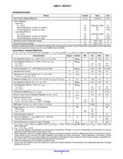
电气规格在P2
型号编号列表在P2
导航目录
LM317BTG数据手册
Page:
of 13 Go
若手册格式错乱,请下载阅览PDF原文件
© Semiconductor Components Industries, LLC, 2016
October, 2019 − Rev. 16
1 Publication Order Number:
LM317/D
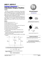
LM317, NCV317
Voltage Regulator -
Adjustable Output, Positive
1.5 A
The LM317 is an adjustable 3−terminal positive voltage regulator
capable of supplying in excess of 1.5 A over an output voltage range of
1.2 V to 37 V. This voltage regulator is exceptionally easy to use and
requires only two external resistors to set the output voltage. Further, it
employs internal current limiting, thermal shutdown and safe area
compensation, making it essentially blow−out proof.
The LM317 serves a wide variety of applications including local, on
card regulation. This device can also be used to make a programmable
output regulator, or by connecting a fixed resistor between the
adjustment and output, the LM317 can be used as a precision current
regulator.
Features
• Output Current in Excess of 1.5 A
• Output Adjustable between 1.2 V and 37 V
• Internal Thermal Overload Protection
• Internal Short Circuit Current Limiting Constant with Temperature
• Output Transistor Safe−Area Compensation
• Floating Operation for High Voltage Applications
• Eliminates Stocking many Fixed Voltages
• Available in Surface Mount D
2
PAK−3, and Standard 3−Lead
Transistor Package
• NCV Prefix for Automotive and Other Applications Requiring
Unique Site and Control Change Requirements; AEC−Q100
Qualified and PPAP Capable
• These Devices are Pb−Free, Halogen Free/BFR Free and are RoHS
Compliant
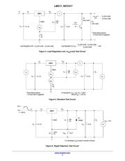
Figure 1. Standard Application
**C
in
is required if regulator is located an appreciable distance from power supply filter.
**C
O
is not needed for stability, however, it does improve transient response.
Since I
Adj
is controlled to less than 100 mA, the error associated with this term is
negligible in most applications.
V
out
+ 1.25V
ǒ
1 )
R
2
R
1
Ǔ
)I
Adj
R
2
LM317
V
in
V
out
R
1
240
R
2
Adjust
I
Adj
C
in
*
0.1 mF
+
C
O
**
1.0 mF
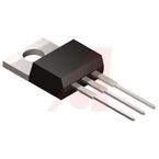
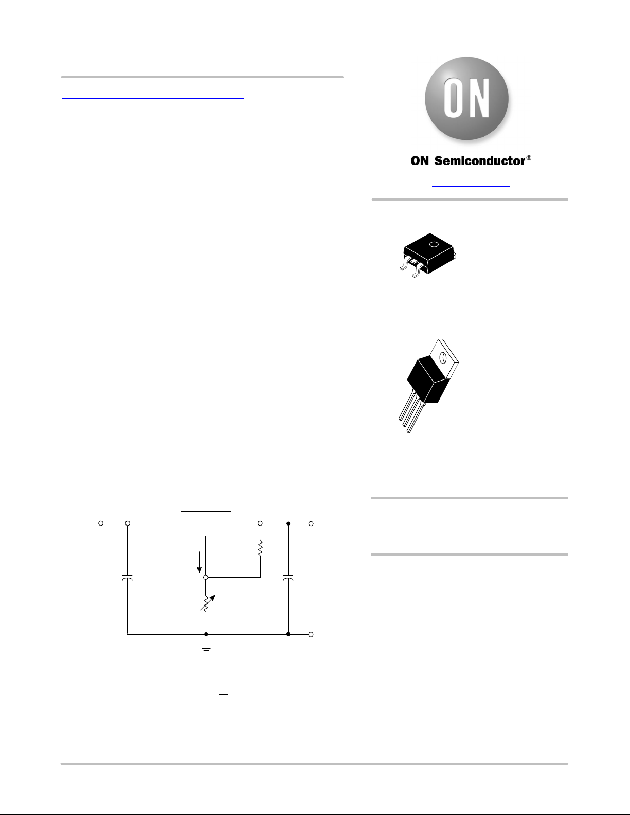
TO−220
T SUFFIX
CASE 221AB
Pin 1. Adjust
2. V
out
3. V
in
D
2
PAK−3
D2T SUFFIX
CASE 936
Heatsink surface (shown as terminal 4 in
case outline drawing) is connected to Pin 2.
3
1
2
Heatsink surface connected to Pin 2.
3
1
2
www.onsemi.com
See detailed ordering and shipping information in the package
dimensions section on page 10 of this data sheet.
ORDERING INFORMATION
See general marking information in the device marking
section on page 10 of this data sheet.
DEVICE MARKING INFORMATION
器件 Datasheet 文档搜索
AiEMA 数据库涵盖高达 72,405,303 个元件的数据手册,每天更新 5,000 多个 PDF 文件
