Datasheet 搜索 > TI(德州仪器) > LSF0108-Q1 数据手册 > LSF0108-Q1 其他数据使用手册 1/24 页

¥ 0
LSF0108-Q1 其他数据使用手册 - TI(德州仪器)
制造商:
TI(德州仪器)
描述:
汽车类 8 通道双向多电压转换器
Pictures:
3D模型
符号图
焊盘图
引脚图
产品图
页面导航:
引脚图在P3Hot
典型应用电路图在P10P11
原理图在P8
封装尺寸在P18P20P21
标记信息在P18
封装信息在P17P18P19P20P21
技术参数、封装参数在P4
应用领域在P1P24
电气规格在P5
导航目录
LSF0108-Q1数据手册
Page:
of 24 Go
若手册格式错乱,请下载阅览PDF原文件
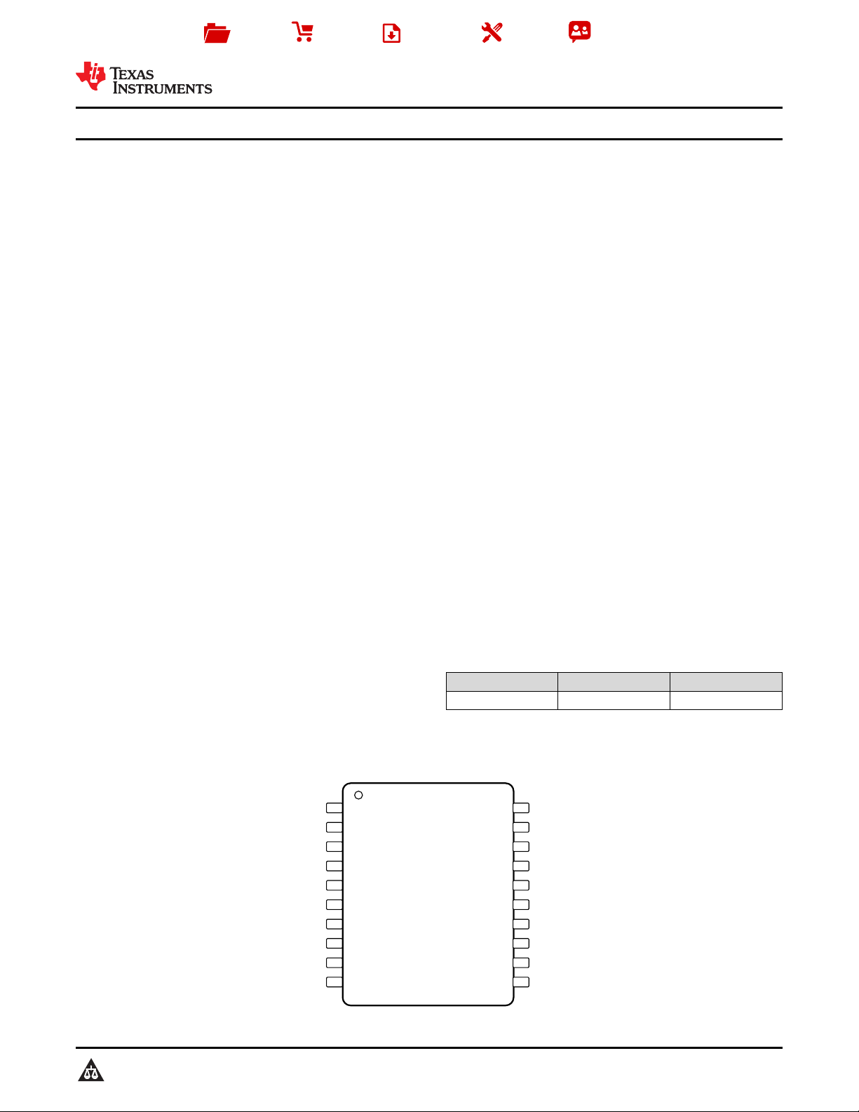
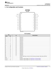
1GND 20 EN
2Vref_A 19 Vref_B
3A1 18 B1
4A2 17 B2
5A3 16 B3
6A4 15 B4
7A5 14 B5
8A6 13 B6
9A7 12 B7
10A8 11 B8
Copyright © 2016, Texas Instruments Incorporated
Product
Folder
Sample &
Buy
Technical
Documents
Tools &
Software
Support &
Community
An IMPORTANT NOTICE at the end of this data sheet addresses availability, warranty, changes, use in safety-critical applications,
intellectual property matters and other important disclaimers. PRODUCTION DATA.
LSF0108-Q1
SDLS967B –MAY 2016–REVISED JUNE 2016
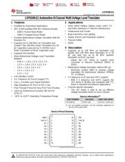
LSF0108-Q1 Automotive 8-Channel Multi-Voltage Level Translator
1
1 Features
1
• Qualified for Automotive Applications
• AEC-Q100 Qualified With the Following Results:
– 2000-V Human-Body Model
– 1000-V Charged-Device Model
• Provides Bidirectional Voltage Translation With No
Direction Pin
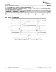
• Supports Up To 100 MHz Up Translation and
Greater Than 100 MHz Down Translation at ≤ 30-
pF Capacitive Load and Up To 40 MHz Up or
Down Translation at 50-pF Capacitive Load
• Supports Hot Insertion
• Allow Bidirectional Voltage Level Translation
Between
– 0.95 V ↔ 1.8 V, 2.5 V, 3.3 V, 5 V
– 1.2 V ↔ 1.8 V, 2.5 V, 3.3 V, 5 V
– 1.8 V ↔ 2.5 V, 3.3 V, 5 V
– 2.5 V ↔ 3.3 V, 5 V
– 3.3 V ↔ 5 V
• Low Standby Current
• 5-V Tolerance I/O Port to Support TTL
• Low r
on
Provides Less Signal Distortion
• High-Impedance I/O Pins For EN = Low
• Flow-Through Pinout for Easy PCB Trace Routing
• Latch-Up Performance Exceeds 100 mA Per
JESD 17
• –40°C to +125°C Operating Temperature Range
2 Applications
• GPIO, MDIO, PMBus, SMBus, SDIO, UART, I
2
C,
and Other Interfaces in Telecom Infrastructure
• Infotainment and Cluster
• Body Electronics and Lighting
• Hybrid, Electric and Powertrain systems
• Passive Safety
• ADAS
3 Description
• Supports up to 100 MHz up translation and
greater than 100 MHz down translation at <= 30
pF cap load and up to 40 MHz up/down
translation at 50 pF cap load:
– Allows the LSF family to support more
consumer or telecom interfaces (MDIO or
SDIO).
• Bidirectional voltage translation without DIR pin:
– Minimizes system effort to develop voltage
translation for bidirectional interface (PMBus,
I
2
C, or SMbus).
• 5 V tolerance on IO port and 125°C support:
– With 5 V tolerance and 125°C support, the
LSF family is flexible and compliant with TTL
levels in industrial and telecom applications.
• Channel specific translation:
– The LSF family is able to set up different
voltage translation levels on each channel.
Device Information
(1)
PART NUMBER PACKAGE BODY SIZE (NOM)
LSF0108-Q1 TSSOP (20) 4.40 mm × 6.50 mm
(1) For all available packages, see the orderable addendum at
the end of the data sheet.
Device Pinout Drawing
器件 Datasheet 文档搜索
AiEMA 数据库涵盖高达 72,405,303 个元件的数据手册,每天更新 5,000 多个 PDF 文件
