Datasheet 搜索 > 双极性晶体管 > ON Semiconductor(安森美) > MJD243T4G 数据手册 > MJD243T4G 其他数据使用手册 1/9 页

¥ 2.159
MJD243T4G 其他数据使用手册 - ON Semiconductor(安森美)
制造商:
ON Semiconductor(安森美)
分类:
双极性晶体管
封装:
TO-252-3
描述:
ON SEMICONDUCTOR MJD243T4G Bipolar (BJT) Single Transistor, NPN, 100 V, 40 MHz, 12.5 W, 4 A, 15 hFE 新
Pictures:
3D模型
符号图
焊盘图
引脚图
产品图
页面导航:
导航目录
MJD243T4G数据手册
Page:
of 9 Go
若手册格式错乱,请下载阅览PDF原文件
© Semiconductor Components Industries, LLC, 2013
September, 2016 − Rev. 17
1 Publication Order Number:
MJD243/D
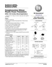
MJD243(NPN),
MJD253(PNP)
Complementary Silicon
Plastic Power Transistors
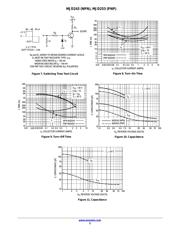
DPAK−3 for Surface Mount Applications
Designed for low voltage, low−power, high−gain audio amplifier
applications.
Features
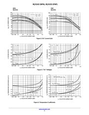
• High DC Current Gain
• Lead Formed for Surface Mount Applications in Plastic Sleeves
(No Suffix)
• Straight Lead Version in Plastic Sleeves (“−1” Suffix)
• Low Collector−Emitter Saturation Voltage
• High Current−Gain − Bandwidth Product
• Annular Construction for Low Leakage
• Epoxy Meets UL 94 V−0 @ 0.125 in
• NJV Prefix for Automotive and Other Applications Requiring
Unique Site and Control Change Requirements; AEC−Q101
Qualified and PPAP Capable
• These Devices are Pb−Free, Halogen Free/BFR Free and are RoHS
Compliant
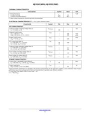
MAXIMUM RATINGS
Rating Symbol Value Unit
Collector−Base Voltage V
CB
100 Vdc
Collector−Emitter Voltage V
CEO
100 Vdc
Emitter−Base Voltage V
EB
7.0 Vdc
Collector Current − Continuous I
C
4.0 Adc
Collector Current − Peak I
CM
8.0 Adc
Base Current I
B
1.0 Adc
Total Device Dissipation
@ T
C
= 25°C
Derate above 25°C
P
D
12.5
0.1
W
W/°C
Total Device Dissipation
@ T
A
= 25°C (Note 2)
Derate above 25°C
P
D
1.4
0.011
W
W/°C
Operating and Storage Junction
Temperature Range
T
J
, T
stg
−65 to +150 °C
ESD − Human Body Model HBM 3B V
ESD − Machine Model MM C V
Stresses exceeding those listed in the Maximum Ratings table may damage the
device. If any of these limits are exceeded, device functionality should not be
assumed, damage may occur and reliability may be affected.
1. When surface mounted on minimum pad sizes recommended.
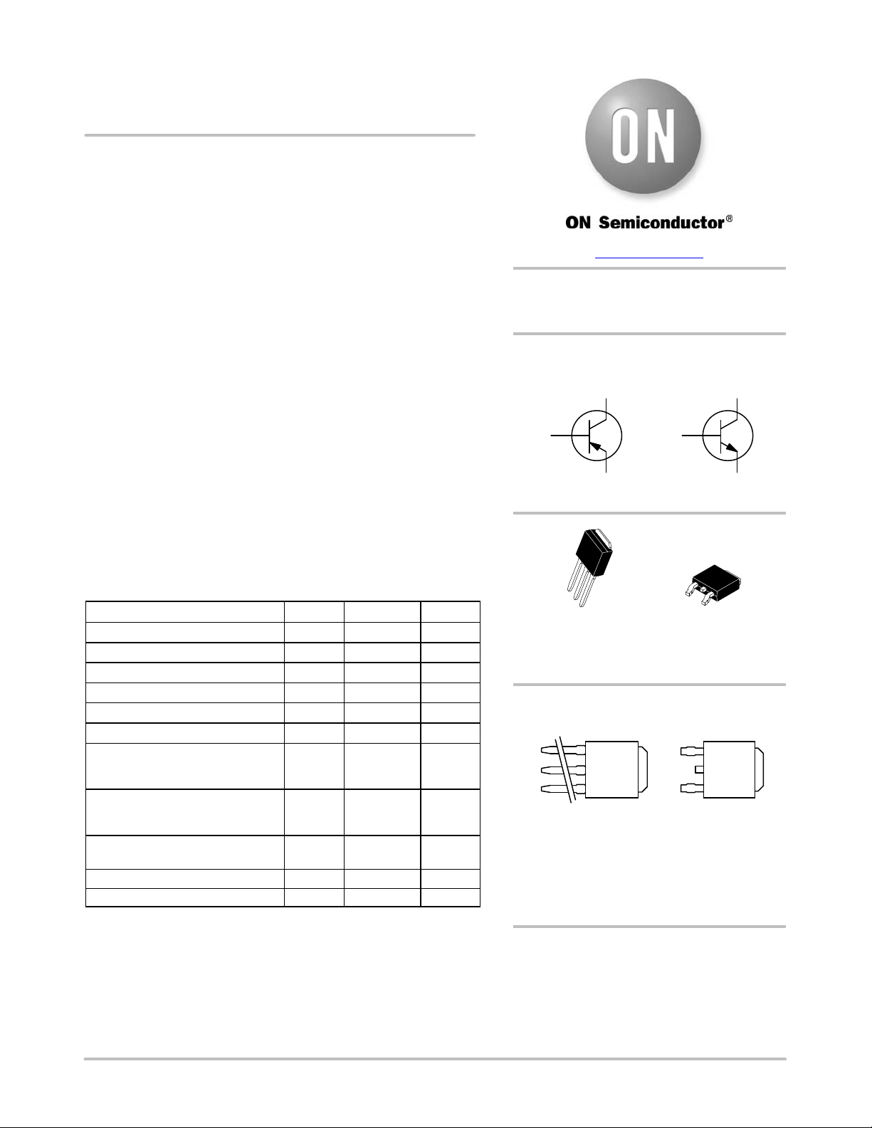
IPAK
CASE 369D
STYLE 1
4.0 A, 100 V, 12.5 W
POWER TRANSISTOR
MARKING DIAGRAMS
A = Assembly Location
Y = Year
WW = Work Week
x = 4 or 5
G = Pb−Free Package
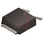
DPAK−3
CASE 369C
STYLE 1
www.onsemi.com
AYWW
J2x3G
AYWW
J253G
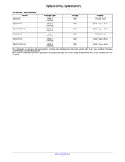
See detailed ordering and shipping information in the package
dimensions section on page 6 of this data sheet.
ORDERING INFORMATION
DPAKIPAK
COMPLEMENTARY
1
BASE
3
EMITTER
COLLECTOR
2, 4
1
BASE
3
EMITTER
COLLECTOR
2, 4
1
2
3
4
1
2
3
4
器件 Datasheet 文档搜索
AiEMA 数据库涵盖高达 72,405,303 个元件的数据手册,每天更新 5,000 多个 PDF 文件
