Datasheet 搜索 > 时钟缓冲器、驱动器、锁相环 > ON Semiconductor(安森美) > NBSG11MNG 数据手册 > NBSG11MNG 产品设计图 1/2 页
 器件3D模型
¥ 284.651
NBSG11MNG 产品设计图 - ON Semiconductor(安森美)
制造商:
ON Semiconductor(安森美)
分类:
时钟缓冲器、驱动器、锁相环
封装:
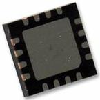
QFN-16
描述:
NBSG 系列 3.3 V 12 GHz 表面贴装 SiGe 1:2 差分 时钟驱动器 - QFN-16
Pictures:
3D模型
符号图
焊盘图
引脚图
产品图
页面导航:
封装尺寸在P1
焊盘布局在P1
标记信息在P1P2
导航目录
NBSG11MNG数据手册
Page:
of 2 Go
若手册格式错乱,请下载阅览PDF原文件
1
ÇÇÇ
ÇÇÇ
ÇÇÇ
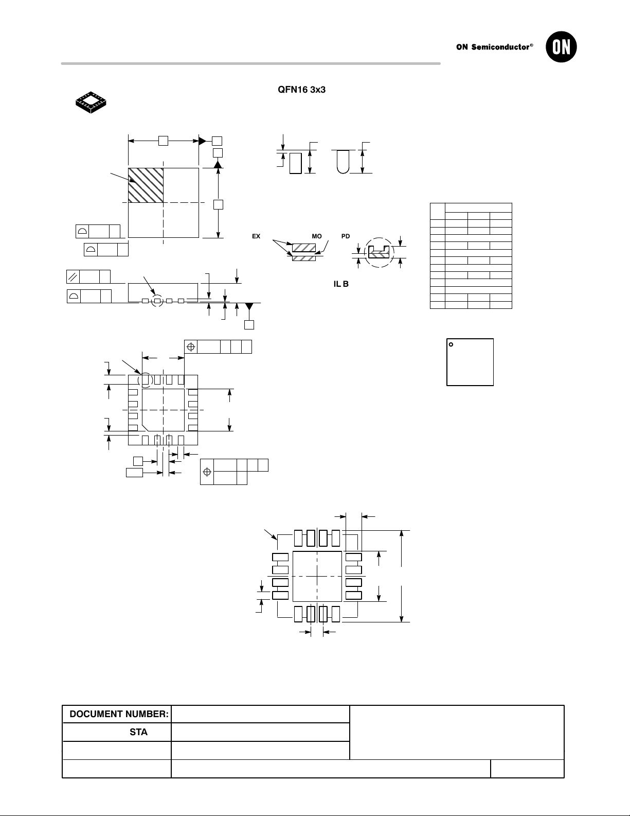
QFN16 3x3, 0.5P
CASE 485G−01
ISSUE F
DATE 22 JUN 2011
SCALE 2:1
16X
SEATING
PLANE
L
D
E
0.10 C
A
A1
e
D2
E2
b
1
4
8
9
16
NOTES:
1. DIMENSIONING AND TOLERANCING PER
ASME Y14.5M, 1994.
2. CONTROLLING DIMENSION: MILLIMETERS.
3. DIMENSION b APPLIES TO PLATED
TERMINAL AND IS MEASURED BETWEEN
0.25 AND 0.30 MM FROM TERMINAL.
4. COPLANARITY APPLIES TO THE EXPOSED
PAD AS WELL AS THE TERMINALS.
B
A
0.10 C
TOP VIEW
SIDE VIEW
BOTTOM VIEW
PIN 1
LOCATION
0.05 C
0.05 C
(A3)
C
NOTE 4
16X
0.10 C
0.05 C
A B
NOTE 3
K
16X
1
L1
DETAIL A
L
ALTERNATE TERMINAL
CONSTRUCTIONS
ÉÉ
ÉÉ
ÇÇ
A1
A3
L
ÉÉ
ÉÉ
DETAIL B
MOLD CMPDEXPOSED Cu
ALTERNATE
CONSTRUCTIONS
DETAIL A
DETAIL B
GENERIC
MARKING DIAGRAM*
XXXXX = Specific Device Code
A = Assembly Location
L = Wafer Lot
Y = Year
W = Work Week
G = Pb−Free Package
XXXXX
XXXXX
ALYWG
G
*This information is generic. Please refer to
device data sheet for actual part marking.
Pb−Free indicator, “G” or microdot “G”,
may or may not be present.
(Note: Microdot may be in either location)
*For additional information on our Pb−Free strategy and soldering
details, please download the ON Semiconductor Soldering and
Mounting Techniques Reference Manual, SOLDERRM/D.
RECOMMENDED
2X
0.50
PITCH
1.84
3.30
1
DIMENSIONS: MILLIMETERS
0.58
16X
2X
0.30
16X
OUTLINE
PACKAGE
2X
2X
0.10 C A B
e/2
SOLDERING FOOTPRINT*
DIM MIN NOM MAX
MILLIMETERS
A 0.80 0.90 1.00
A1 0.00 0.03 0.05
A3 0.20 REF
b 0.18 0.24 0.30
D 3.00 BSC
D2 1.65 1.75 1.85
E 3.00 BSC
E2 1.65 1.75 1.85
e 0.50 BSC
K 0.18 TYP
L 0.30 0.40 0.50
L1 0.00 0.08 0.15
MECHANICAL CASE OUTLINE
PACKAGE DIMENSIONS
http://onsemi.com
1
© Semiconductor Components Industries, LLC, 2002
October, 2002 − Rev. 0
Case Outline Number:
XXX
DOCUMENT NUMBER:
STATUS:
NEW STANDARD:
DESCRIPTION:
98AON04795D
ON SEMICONDUCTOR STANDARD
QFN16, 3X3 MM, 0.5 PITCH
Electronic versions are uncontrolled except when
accessed directly from the Document Repository. Printed
versions are uncontrolled except when stamped
“CONTROLLED COPY” in red.
PAGE 1 OF 2
器件 Datasheet 文档搜索
AiEMA 数据库涵盖高达 72,405,303 个元件的数据手册,每天更新 5,000 多个 PDF 文件
