Datasheet 搜索 > TVS二极管 > ST Microelectronics(意法半导体) > P6KE18A 数据手册 > P6KE18A 产品封装文件 1/5 页

¥ 1.271
P6KE18A 产品封装文件 - ST Microelectronics(意法半导体)
制造商:
ST Microelectronics(意法半导体)
分类:
TVS二极管
封装:
DO-15
描述:
STMICROELECTRONICS P6KE18A TVS二极管, Transil P6KE系列, 单向, 15.3 V, 32.5 V, DO-15, 2 引脚
Pictures:
3D模型
符号图
焊盘图
引脚图
产品图
页面导航:
导航目录
P6KE18A数据手册
Page:
of 5 Go
若手册格式错乱,请下载阅览PDF原文件
© Semiconductor Components Industries, LLC, 2009
October, 2009 − Rev. 10
1 Publication Order Number:
P6KE6.8A/D
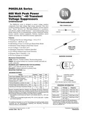
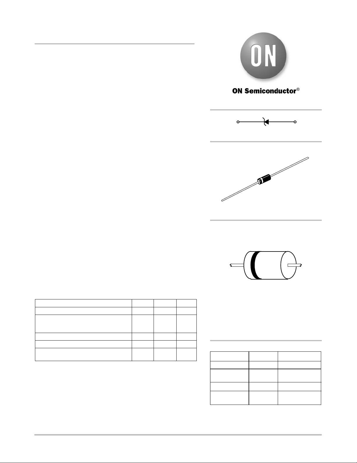
P6KE6.8A Series
600 Watt Peak Power
Surmetict-40 Transient
Voltage Suppressors
Unidirectional*
The P6KE6.8A series is designed to protect voltage sensitive
components from high voltage, high energy transients. They have
excellent clamping capability, high surge capability and fast response
time. These devices are ON Semiconductor’s exclusive,
cost-effective, highly reliable Surmetic axial leaded package and is
ideally-suited for use in communication systems, numerical controls,
process controls, medical equipment, business machines, power
supplies and many other industrial/consumer applications.
Features:
• Working Peak Reverse Voltage Range − 5.8 to 171 V
• Peak Power − 600 W @ 1 ms
• ESD Rating of Class 3 (>16 KV) per Human Body Model
• Maximum Clamp Voltage @ Peak Pulse Current
• Low Leakage < 5 mA above 10 V
• Maximum Temperature Coefficient Specified
• UL 497B for Isolated Loop Circuit Protection
• Response Time is Typically < 1 ns
• Pb−Free Packages are Available*
Mechanical Characteristics:
CASE:
Void-free, Transfer-molded, Thermosetting plastic
FINISH: All external surfaces are corrosion resistant and leads are
readily solderable
MAXIMUM LEAD TEMPERATURE FOR SOLDERING:
260C, 1/16″ from the case for 10 seconds
POLARITY: Cathode indicated by polarity band
MOUNTING POSITION: Any
MAXIMUM RATINGS
Rating Symbol Value Unit
Peak Power Dissipation (Note 1) @ T
L
≤ 25°C P
PK
600 W
Steady State Power Dissipation
@ T
L
≤ 25°C, Lead Length = 3/8 in
Derated above T
L
= 50°C
P
D
5.0
50
W
mW/°C
Thermal Resistance, Junction−to−Lead
R
q
JL
20 °C/W
Forward Surge Current (Note 2) @ T
A
= 25°C I
FSM
100 A
Operating and Storage Temperature Range T
J
, T
stg
− 55 to
+150
°C
Stresses exceeding Maximum Ratings may damage the device. Maximum
Ratings are stress ratings only. Functional operation above the Recommended
Operating Conditions is not implied. Extended exposure to stresses above the
Recommended Operating Conditions may affect device reliability.
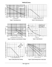
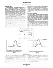
1. Nonrepetitive current pulse per Figure 4 and derated above T
A
= 25°C per
Figure 2.
2. 1/2 sine wave (or equivalent square wave), PW = 8.3 ms, duty cycle = 4 pulses
per minute maximum.
*For additional information on our Pb−Free strategy and soldering details, please
download the ON Semiconductor Soldering and Mounting Techniques
Reference Manual, SOLDERRM/D.
http://onsemi.com
Cathode Anode
MARKING DIAGRAM
A
P6KE
xxxA
YYWW
Device Package Shipping
†
ORDERING INFORMATION
P6KExxxA Axial Lead 1000 Units / Box
P6KExxxAG Axial Lead
(Pb−Free)
1000 Units / Box
†For information on tape and reel specifications,
including part orientation and tape sizes, please
refer to our Tape and Reel Packaging Specifications
Brochure, BRD8011/D.
P6KExxxARL Axial Lead 4000/Tape & Reel
P6KExxxARLG Axial Lead
(Pb−Free)
4000/Tape & Reel
AXIAL LEAD
CASE 017AA
PLASTIC
A = Assembly Location
P6KExxxA = Device Number
YY = Year
WW = Work Week
= Pb−Free Package
(Note: Microdot may be in either location)
器件 Datasheet 文档搜索
AiEMA 数据库涵盖高达 72,405,303 个元件的数据手册,每天更新 5,000 多个 PDF 文件
